Anisotropic Conducting Film (ACF) of Ag Nanoparticles as Transfer Polymer and Electrical Interface for Silicon Micro- an
- PDF / 382,698 Bytes
- 6 Pages / 432 x 648 pts Page_size
- 92 Downloads / 254 Views
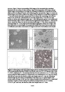
Anisotropic Conducting Film (ACF) of Ag Nanoparticles as Transfer Polymer and Electrical Interface for Silicon Micro- and Nano- Pillars Matthew Ombaba, Logeeswaran V. J and M. Saif Islam Department of Electrical and Computer Engineering, University of California-Davis, CA 95616 ABSTRACT We report a novel application of Anisotropic Conductive Films (ACFs) technology to provide electrical contact and mechanical anchor between fracture transfer-printed (1-D) single crystal semiconductor micro- and nanopillars and a bottom metal. This fracture-transfer method enables highly crystalline micro- and nanopillars of different materials with diverse bandgaps and physical properties to be fabricated on appropriate mother substrates and transferred to form multilayered 3D stacks for multifunctional devices. The proposed protocol incorporates silver (Ag) nanoparticles into thermoplastic polymers exploitable in transfer-printed semiconductor devices and circuits with low contact resistance that is compatible with current IC processing methods. The vertical micropillars arrays are then embossed onto the polymer at its rubbery state by applying a vertical force leading to particle trapping between the bottom electrode and the micropillars. The polymer is then hardened while retaining the applied vertical force. By applying a lateral force on the mother substrate, the firmly cemented pillars are fractured off thereby allowing the mother substrate to be reused. INTRODUCTION There has been immense interest in semiconductor based nanowires and nanopillars prepared from both top-down and bottom-up approaches across the scientific and manufacturing communities as a result of their unique properties that more often than not differ from those of their traditional bulk counterparts. In particular, achievements have been attained in preparing various nanoarrays of semiconductor materials in a controllable and ordered manner. For example, alumina templates have been used to control the spacing, length and thicknesses of several semiconductor nanowire arrays with great success as a bottom-up approach. Further, the semiconductor industry has a well-established top down lithographical approach to the preparation of semiconductor nano and microwires of different shapes on a wide variety of wafers using both wet and dry etchants while bottom-up routes have also been utilized in conjunction with different deposition techniques to realize the same result. However, the substrates have almost always been metallic, ceramic or semiconductor in nature. Little has been achieved in their transfer to cheap and plastic substrates while at the same time maintaining their crystallinity, order and integrity. A. Javey and group have demonstrated a viable route to large scale contact and rollprinting of semiconductor nanowire parallel arrays on secondary receiver substrates like different plastic materials, paper and glasses, other than those they were prepared on or their mother substrates in a horizontal orientation1. Consequently, they have demonstrated a few
Data Loading...