Electrical Contact Characteristics between Silicon Micropillars and Ag Nanoparticles with Controlled Mechanical Load
- PDF / 649,080 Bytes
- 5 Pages / 612 x 792 pts (letter) Page_size
- 46 Downloads / 283 Views
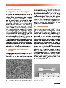
Electrical Contact Characteristics between Silicon Micropillars and Ag Nanoparticles with Controlled Mechanical Load Logeeswaran VJ1, Mark Triplett1,2, Daniel Lam1, Emre Yengel1, Heim Grewal1, Matthew Ombaba1 & M. Saif Islam1 1
Department of Electrical and Computer Engineering, University of California-Davis, CA 95616.
2
Department of Physics, University of California-Davis, CA 95616.
ABSTRACT We report an experimental investigation on employing Ag nanoparticles to provide electrical and mechanical contacts between transfer-printed semiconductor devices in the shape of micro/nano- wires and pillars. The Ag nanoparticles have diameters ranging between 200800nm and are assembled on a 200nm Au film deposited on glass substrates. With a customized tool, an ensemble of silicon pillars were brought into contact with the silver (Ag) nanoparticles (AgNPs) by precisely controlling the displacement and applied force (pressure). Current-voltage measurements were done at force resolution of ~0.2N. The test method aims to illuminate the pillar-particle contact mechanism using the nanoparticles as conductive fillers for the next generation of high performance heteroepitaxial device transfer-printing applications.
INTRODUCTION There have been various approaches developed over the last decades for heterogeneous integration of single crystal semiconductors (e.g. Si, InP, GaAs etc.) with different physical, electrical and optical characteristics on a single substrate. Some of the integration methods that have been demonstrated include wafer bonding [1-2], epitaxial liftoff [3-5], direct growth [6, 7] and transfer printing [8-10]. Heterogeneous integration has been facilitated by the introduction of structures in the form of crystalline semiconductor micro/nano- wires/pillars/rods as the active materials. The structures have unique properties that are advantageous, for example, in photovoltaic devices, such as light trapping, charge separation, and charge transport. In a bottomup approach, the device fabrication can be achieved by directly growing the active crystalline micro/nano-structures on the final substrate (also the growth substrate) or by transfer printing the micro/nano-structures from the growth substrate to a low cost carrier substrate. For the top-down approach, the micro/nano-structures are formed using wet or dry etching techniques. The use of direct growth methods is limited to growth substrates that are compatible with the conventional high temperature microfabrication processes such as quartz substrates [6] and refractory metal foils [7]. This is in contrast to transfer printing techniques that enable rigid, planar and brittle semiconductors for numerous applications in electronics and photonics, to be processed near room temperature on flexible, low cost substrates, such as plastic, glass or metal sheets. Transfer printing techniques in literature have been mostly limited to 2-dimensional (2D) single crystal film transfer with some exceptions [11, 12]. Forming multiple terminal electrical contacts to the transf
Data Loading...