Arsenic Implant Activation and Redistribution in P-Type Silicon Induced by Pulsed Electron Beam Annealing
- PDF / 253,512 Bytes
- 6 Pages / 420.48 x 639 pts Page_size
- 7 Downloads / 369 Views
ARSENIC IMPLANT ACTIVATION AND REDISTRIBUTION IN P-TYPE SILICON INDUCED BY PULSED ELECTRON BEAM ANNEALING D. BARBIER+, M. BAGHDADI+, A. LAUGIER+ and A. CACHARD++ + : Laboratoire de Physique de la Mati~re, Institut National des Sciences Appliqu6es de Lyon, 20 Avenue Albert Einstein 69621 VILLEURBANNE CEDEX (France) ++ : D6partement de Physique des Mat~riaux, Universit6 Claude Bernard-Lyon I 43, Boulevard du 11 Novembre 1918, 69622 VILLEURBANNE CEDEX (France)
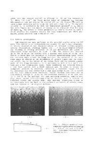
ABSTRACT In this work Pulsed Electron Beam Annealing has been used to Sctivaye As implanted in (100) and (Ill) silicon (140 keV10 cm- ). With a selected electron beam energy deposition profile excellent regrowth layer 2uality and As activation has been obtained in the 1.2-1.4 J/cm fluence range. As redistribution isconistent with the melting model assuming a diffusivity of 10 cm /s in liquid silicon. As losses might slightly reduce the carrier concentration near the surface in the case of (100) silicon. However a shallow and highly active N+ layer have been achieved with optimized PEBA conditions. 1. INTRODUCTION Ion implantation followed by a single submicrosecond high energy pulse is now considered as among the most attractive doping process for shallow junction formation in silicon. Implant activation is obtained by liquid phase epitaxial regrowth of the amorphous surface layer starting from the undamaged substrate. In past years pulsed laser annealing has been widely used to activate most of the classical dopants in silicon with various implantation parameters (1). A few works have been devoted to pulsed electron beam annealing (PEBA) up to now, but it has been recently demonstrated that this technique can be successfully used to achieve shallow implanted junctions in silicon solar cells (2)(3). However, as well as with any other pulsed beam technique, annealing kinetics must be optimized as a function of implantation parameters. Desired doping profiles can only be obtained by controlling thermal effects of the pulse (molten layer thickness, melt front velocity, temperature profiles). This is made easier in the case of electrons than in the case of lasers because the heat generation function in the material can be largely modified by variation of acceleration voltages and beam currents. In this work an optimized electron beam pulse has been used with vfious Iluences to recrystallize p-type (100) and (Ill) silicon implanted with arsenic (10 /cm -140 keV). RBS and SIMS were used to study annealing effects. Dopant activation has been investigated by mean of incremental sheet resistance measurements. 2. EXPERIMENT The machine used for annealing (SPIRE-300) has been described in ref.3. It allows for adjustment of electron beam parameters (energietscurrents, annealing diameter). These have been selected to yield an energy deposition profile convenient for melting the silicon surface over a few tenths of microns with a pulse duration of about 50 ns. The mean electron energy has been kept around 15 KeV and the samples have been processed in a Mat.
Res.
Soc.
Symp
Data Loading...