Atomic Structure, Band Offsets and Hydrogen in High K oxide:Silicon interfaces
- PDF / 1,244,361 Bytes
- 13 Pages / 595 x 842 pts (A4) Page_size
- 52 Downloads / 285 Views
N7.5.1/T5.5.1
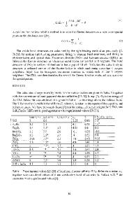
Atomic Structure, Band Offsets and Hydrogen in High K oxide:Silicon interfaces J Robertson* and P W Peacock Engineering Department, Cambridge University, Cambridge CB2 1PZ, UK * [email protected] Abstract The bonding, electronic structure and valence band offsets are calculated for various atomic models of interfaces between Si and high dielectric constant insulators ZrO2 and SrTiO3. A non-polar face of the oxide does not necessarily give a semiconducting interface, because of the need to fill Si dangling bond states on the Si side. This can be achieved by stoichiometry changes. Band offsets of semiconducting interfaces are generally the same as those found from bulk charge neutrality levels, indicating no dipole layers. Dipole layers are present at some configurations, where the offset is then changed by up to 1 eV. The states of hydrogen in the oxides are also considered. Introduction The decrease of dimensions of CMOS transistors has led to the need for alternative, high dielectric constant (κ) oxides to replace silicon dioxide as a gate dielectric [1]. The oxides must satisfy various requirements. They should be stable in contact with Si to withstand high temperature processing. They should act as a potential barrier to both electrons and holes, which requires a combination of the band offsets and tunnelling mass to be large enough [2,3]. They should not have low frequency polar phonon modes [4], which scatter carriers. They should form a high quality interface in contact with silicon, with a low density of interfacial defects. A good interface requires either that the oxide is amorphous, or that it is epitaxial and lattice-matched to the underlying silicon. Amorphous oxides are one low-cost solution, as they are expected to be able to adjust its local bonding to minimise the number of Si dangling bonds at the interface. The alternative is to use an epitaxial oxide. This involves more effort, but it has an advantage scientifically as it allows us to investigate some of the underlying problems in detail. It has been possible to grow SrTiO3, Y-stabilised ZrO2, and (La,Y)2O3 epitaxially on Si [5-10]. LaAlO3 is also closely lattice matched to Si. The lattice constant of Si and ZrO2 and Si are 5.43Å and 5.07Å respectively, which allows growth on a (100) face with ZrO2(100)//Si(100) and ZrO2[001]//Si[001]. Y2O3 has the cubic bixbyite structure with a=10.6Å. Alloying with La2O3 reduces the lattice constant to allow a lattice match with Si, and growth on Si(111)[9]. The lattice constant SrTiO3 and LaAlO3 are 3.90Å and 3.78Å respectively, so that lattice match is possible on Si(100) with SrTiO3[110]//Si[100] with a 450 rotation of the SrTiO3 lattice [5]. Strictly, SrTiO3 is not the best oxide, because its conduction band offset is too low, but it is considered because its technology is most advanced. We previously calculated the band offsets of the various oxides against silicon using the method of charge neutrality levels (CNL)[2]. This matches the CNL of the bulk oxide to that of the bulk Si. It appears t
Data Loading...