Barriers Against Copper Diffusion into Silicon and Drift Through Silicon Dioxide
- PDF / 2,530,186 Bytes
- 11 Pages / 576 x 777.6 pts Page_size
- 54 Downloads / 271 Views
a three metal level interconnect structure using Cu as the conductive material. The interlevel dielectrics (ILD) could be conventional SiO2-based materials or more ideally, materials with low dielectric constants such as polyimide. If conventional SiO2 is used, then Cu plugs and interconnects have to be enclosed in diffusion/ drift barriers so that Cu will not move into Si or SiO2 under thermal stress or biased temperature stress (BTS). This article reviews the published studies on conductive diffusion barriers between thin Cu films and Si substrates. In addition, the work on diffusion and drift of Cu into commonly used inorganic dielectric systems is also summarized. Finally, some concerns involving diffusion/ drift barriers between Cu and Si or SiO2 for sub-0.5 /xm feature size with high aspect ratios are discussed.
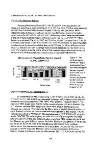
Si/Conductive Diffusion Barrier/Cu
Figure 1. Cross-sectional diagram of a three metal level interconnect structure using Cu as the conductor.
30
After an extensive literature search, 46 papers, mainly from U.S. science and technology journals, could be found. The diffusion barriers studied can be classified into six groups: (1) polycrystalline transition metal barriers; (2) polycrystalline or amorphous transition metal alloy barriers; (3) polycrystalline or amorphous transition metal-silicon (including silicide) barriers; (4) polycrystalline or amorphous transition metal-nitrogen (including nitride), -oxygen (including conductive oxide), and -boron (boride) barriers; (5) amorphous ternary barriers; and (6) amorphous carbon barri-
ers. In the following sections, the sample preparation methods and the experimental results will be summarized. The failure mechanisms for different types of diffusion barriers are discussed.
Sample Preparation and Analytical Techniques Most investigations were done on unpatterned Si (or occasionally on silicided Si) substrates. The common sample preparation procedure involved degreasing Si substrates in organic solvents and stripping the native oxide in a dilute HF solution before diffusion barrier/Cu deposition. For most depositions of diffusion barriers, conventional physical vapor deposition (PVD) of either sputtering in an inert gas, or reactive sputtering in a mixture of inert and reactive gases, or e-beam evaporation were used. Six out of 46 studies employed a CVD technique to deposit the barrier films, such as CVD W " CVD TiN,45 and CVD TiB2.6 Cu films were almost exclusively deposited by conventional PVD techniques, except three studies7"9 that used CVD Cu deposition. The barrier/Cu structures were made either with or without breaking vacuum between the deposition of each layer. In the PVD systems, the base pressure ranged from low 10 " 6 to low 10 ~8 torr, while the deposition pressure for the sputtering processes varied in the range of 2 to 30 mtorr at powers from 0.3 to 3 kW or at rates from 0.3 to 50 A/s. Intentional substrate heating and substrate bias were seldom applied. The pressures for CVD were usually higher (up to 15 torr). After deposition, these u
Data Loading...