Boron Doping Effects in Microcrystalline Silicon
- PDF / 877,982 Bytes
- 6 Pages / 612 x 792 pts (letter) Page_size
- 100 Downloads / 476 Views
0989-A07-07
Boron Doping Effects in Microcrystalline Silicon Wolfhard Beyer, Lars Niessen, and Frank Pennartz IEF-5 Photovoltaik, Forschungszentrum J¸lich GmbH, Leo Brandt Strasse, J¸lich, 52425, Germany ABSTRACT Conditions leading to high conductivities (up to 300 S/cm) in chlorosilane-based borondoped microcrystalline Si:Cl:H films are investigated. It is found that the high conductivity originates primarily from the growth of highly crystalline material with a high concentration of boron. Furthermore, these films grow with relatively low chlorine and hydrogen concentrations of a few percent and, according to effusion measurements of hydrogen and implanted helium, in a relatively compact structure. At a boron doping level of 1%, admixture of 10% silane to the tetrachlorosilane results in the growth of amorphous material of low conductivity while for admixture of up to 90% of silicontetrafluoride, microcrystalline Si films with high conductivities can be grown.
INTRODUCTION Highly conductive microcrystalline silicon films are of interest for application as contact layers in microcrystalline silicon thin film solar cells. However, in the standard silane (SiH4) based technology, an asymmetry is observed for p- and n-type doping. Highest conductivities reached by boron doping are found to be more than a factor of 10 lower than those obtained by phosphorus doping, where maximum conductivities lie in the range of 100 (Ωcm)-1 [1,2]. Recently we found high conductivity values for boron-doped microcrystalline Si films prepared by plasma-enhanced chemical vapour deposition (PECVD) from tetrachlorosilane-hydrogendiborane gas mixtures [3, 4, 5]. Room temperature conductivities of nearly 300 (Ωcm)-1 were obtained [4]. In this article we investigate the peculiarities of this B-doped chlorinated material and explore to what degree such high conductivities can be reached by using gas mixtures of chlorosilane with silane or silicontetrafluoride.
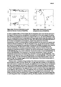
EXPERIMENTAL DETAILS The films were prepared by plasma deposition (PECVD) employing the same regime as applied previously [3-5], namely a high dilution of SiCl4 /SiH4 /SiF4 in hydrogen, a rather high pressure of 8 mbar (measured by a baratron) and a high rf (13.56 MHz) power of 40 -60 W (0.7 1W/cm2). A hydrogen flow of 100 to 300 sccm and a flow of SiCl4 /SiH4 /SiF4 of 1 to 8 sccm were used. For doping, flows of diborane (B2H6) were added. Typical substrate temperature was TS = 250∞C. As substrates, crystalline silicon and quartz were used. The film thickness ranged between 0.24 and 1.2 µm with typical values near 0.8 µm. For structural characterization (crystallinity), Raman measurements were employed (using the 488 nm line of an argon laser) [6]. The chlorine, fluorine and boron content were analyzed by secondary ion mass spectrometry
(SIMS) while the hydrogen concentration was determined by hydrogen effusion (using a heating rate of 20K/min) measurements. Effusion measurements of implanted He were used for structural characterization. For electrical characterization, dark conductiv
Data Loading...