Channel Epitaxy of 3C-SiC on Si Substrates by CVD
- PDF / 622,433 Bytes
- 8 Pages / 595 x 842 pts (A4) Page_size
- 49 Downloads / 408 Views
K1.2.1
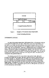
Channel Epitaxy of 3C-SiC on Si Substrates by CVD S. Nishino, Y. Okui, C. Jacob* and S. Ohshima, Kyoto Institute of Technology, Department of Electronics and Information Science, Kyoto, JAPAN; * Materials Science Center, Indian Institute of Technology, Kharagpur, INDIA. Abstract. Epitaxial growth of 3C-SiC on Si substrates has been studied for many years, however an important issue is how to reduce the high density of interfacial defects. Channel epitaxy is the growth of a film on small channeled windows and is related to selective growth. Channel epitaxy of 3C-SiC grown on the seed 3C-SiC previously deposited on patterned Si substrates was achieved via CVD using hexamethyldisilane (HMDS). The proper selection of mask materials was also key to achieve channel epitaxy. Thermal oxide, silicon nitride and thin SiC masks were tried. Thin SiC was an effective mask to achieve selective growth at 1350oC. Smooth surface morphology was observed on both the channel regions and the mask regions at the growth temperature of 1350oC. Scanning electron microscopy revealed coalescence of the laterally grown regions via channel epitaxial growth of 3C-SiC. INTRODUCTION Cubic silicon carbide (3C-SiC) is a desirable material for high mobility devices because of homogeneous effective mass in any direction. It has been necessary to grow 3C-SiC films using heteroepitaxial growth on foreign substrates such as Si since large-area bulk 3C-SiC crystals are not available. 3C-SiC has been grown epitaxially on Si substrates for many years [1]. However, the large lattice mismatch (~20%) induces a large number of defects such as misfit dislocations, twins, stacking faults and threading dislocations at the 3C-SiC/Si interface. Channel epitaxial growth of 3C-SiC on patterned Si substrates is potentially one way to resolve this problem. This method is based on seeded growth in narrow micron size channels and epitaxial lateral overgrowth (ELOG) processes by using an appropriate mask material to prevent the propagation of threading dislocations originating from the 3C-SiC/Si interface. Therefore, lateral overgrowth of a 3C-SiC layer until coalescence results in a 3C-SiC layer of lower defect-density material. Microchannel epitaxy (MCE) followed by the ELOG technique has been reported for GaAs on Si [2]. The technique has been successfully applied to grow 3C-SiC on Si. The above work was done on Si (100) [3,4] and Si (111) substrates [5]. One big issue for 3C-SiC on Si(100) is the appearance of
K1.2.2
APB’s (Anti-Phase Boundary’s). The formation of APB’s during the heteroepitaxial growth of the(100) plane of zinc blend structure on the (100) Si window
plane of diamond structure is well known. The Si(111)
SiO2
plane is preferable to avoid APB’s in 3C-SiC(111), because the (111) substrate is the polar face of 3C-SiC.
(a)
This paper reports on a promising technique of 3C-SiC on patterned Si substrates by applying
(b)
microchannel epitaxy. The following sections describe the experimental parameters necessary to achieve
(c)
3C-SiC film vi
Data Loading...