Channeling Study of Partially Ionized Beam Deposited Epitaxial Ag Films on Si(111) Substrates
- PDF / 365,431 Bytes
- 6 Pages / 420.48 x 639 pts Page_size
- 111 Downloads / 338 Views
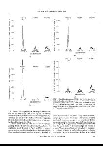
CHANNELING STUDY OF PARTIALLY IONIZED BEAM DEPOSITED EPITAXIAL Ag FILMS ON Si(111) SUBSTRATES H.-S.J1IN*, L. You** and T.-M.Lu** *Department of Physics, Brooklyn College of The City University of New York, Brooklyn, New York, 11210. ** The Center for Integrated Electronics and Physics Department, Rensselaer Polytechnic Institute, Troy, NY 12181. ABSTRACT Ag films deposited on Si(111) substrates by partially ionized beam (PIB) under conventional vacuum conditions were studied by MeV ion channeling techniques. In spite of their large lattice mismatch (24.8%), Ag films were still found to be epitaxial. With a deposition temperature of 350 0 C and without post-annealing, the Xmin value at the surface of a 2550 Ao thick Ag film was found to be 10%. The azimuthal angular scan and the measured axial channeling dip showed that the Ag film was (11l) oriented. The lattice quality of the films was comaparable to that deposited by MBE techniques. Dislocations were found in the PIB deposited Ag films. Lattice damage due to the bombardment of energetic ions was also observed. The thickness of the Ag film was found to have a pronounced effect on the crystalline quality at the surface. With the thickness increasing from 1240 AO to 2550 AO, the lattice quality at the Ag surface improved significantly, but not much change in the defect density in the Ag films was obseved. I. INTRODUCTION: The growth of epitaxial Al films on silicon wafers to overcome many difficulties in the use of Al for VLSI applications has been of great interest. Since the lattice mismatch between Al and Si is 25.4%, it is also of fundamental interest to see if the Al films can still be epitaxially grown. During the past years, ionized cluster beam (ICB) deposition and other conventional techniques have been used for this purpose [I]. Channeling techniques have been applied to study the structural properties of the ICB deposited Al films on Si [2]. It has been shown that, despite the large lattice mismatch, the Al films are still epitaxial. The epitaxial growth is attributed to the coincidence between the lattices of Al and Si. That is, four Al lattice planes match three Si lattice planes very well, resulting in a very small effective lattice mismatch of 0.6%. This is known as " coincident epitaxial growth". Based on this point of view, Ag films on Si wafers would be another system for coincident growth. The lattice mismatch between Ag and Si is 24.8% and the effective lattice mismatch between them is even smaller, 0.3%. MBE techniques have been used to grow the Ag films [3,4]. Channeling techniques have been used to study the MBE deposited Ag films 13-5]. Similarly, it was shown that the MBE deposited Ag films are also epitaxial. The results 5 on MBE deposited Ag films have also been compared to that on the ICB deposited Al films[ ]. Recently, a noval technique called the partially ionized beam (PIB) deposition has been developed at Rensselaer Polytechnic Institute [6]. It operates in a conventional vacuum of about 10-5 Pa and, similar to ICB deposition, it has
Data Loading...