Electromigration Behavior of Aluminum Films Deposited by Partially Ionized Beam
- PDF / 694,831 Bytes
- 5 Pages / 420.48 x 639 pts Page_size
- 23 Downloads / 343 Views
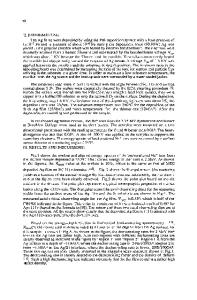
ELECTROMIGRATION BEHAVIOR OF ALUMINUM FILMS DEPOSITED BY PARTIALLY IONIZED BEAM. O.V.KONONENKO,L.K.FIONOVA,AND V.N.MATVEEV Institute of Microelectronics Technology and High Purity Materials of the USSR Academy of Sciences,142432 Chernogolovka, Moscow district,USSR. ABSTRACT Aluminum stressed by a of 3000C. The kV lived over
films deposited by par~ally 2ionized beam were current density of 2x10 A/cm at a temperature films prepared at the acceleration voltage of 5 200 hours.
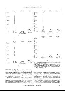
INTRODUCTION Aluminum films are widely used as interconnections in microelectronic devices. One of the most important features of aluminum interconnections is its resistance to damage due to electromigration [1]. Electromigration occurs mainly along grain boundaries (2], therefore, it depends strongly on the microstructure of the films [3]. It is known that ion bombardment during film growth can modify the film structure [4]. A number of investigators have successfully used self-ions for deposition aluminum films with desirable properties [5,6]. We report here the results of lifetime tests of the aluminum films prepared by self-ions-assisted method. EXPERIMENTAL PROCEDURES Unpassivated aluminum filmy were deposited by partially ionized beam in a vacuum 4x10 Torr. The 99.999 at % pure aluminum was vaporized from graphite crucible using electron bombardment heating. The ion/atom ratio a ranged from 5% to 10%, and was estimated from the knowledge of the total current received at the substrate and the deposition rate. The ions were accelerated by a potential of 3 and 5 kV towards the substrate.The film were deposited onto an oxidized (111) single crystal silicon with 4800-4-thick SiO The substrate was unintentionally heated during the deposition by a radiation of the hot crucible to a temperature of less than 50°C. Electromigration test structures were patterned using standard photolithographic procedures and chemical etching. The test stripe length was 540 gm and the stripe width was 10 gm. After patterning the6 stripes were annealed for 1 hour at 0 480 C in a vacuum 10 Torr.The resistivity of films was measured to be 2.7 gicm. Structure of the films was examined by TEM JEM-1000 before and after annealing. The samples for TEM examination were prepared by etching a crater on the back side of the substrate with a mixture of HNO 3 ,HF and CH 3 COOH(10:6:6).
Mat. Res. Soc. Symp. Proc. Vol. 239. @1992 Materials Research Society
714
RESULTS AND DISCUSSION Structural characteristics of the films are listed in TABLE. Furthermore,there are many equilibrium special and lowThey are formed after annealing. angle grain boundaries (GB) during secondary grain growth taking place in the films during annealing [7]. It is known that such GB possess perfect structudere and extremely low energy. They are bad sinks for lattice fects [8]. GB diffusion of such GBs is some order less than one of common GB's [9]. TABLE.
Structural characteristics of the films. as-deposited annealed
Accelerating voltage Average grain size, d(jm)
3kV
5kV
3kV
5kV
0.37
0.085
1.5
Data Loading...