Characterisation of Ion Implanted and Thin Epitaxial Layer Structures Using Photoluminescence
- PDF / 298,992 Bytes
- 7 Pages / 420.48 x 639 pts Page_size
- 66 Downloads / 311 Views
CHARACTERISATION OF ION IMPLANTED AND THIN EPITAXIAL LAYER STRUCTURES USING PHOTOLUMINESCENCE B. Hamilton *, T.O. Sedgwick and J.C. Gelpey t IBM, Thomas J. Watson Research Centre,Yorktown Heights, NY 10598. U.S.A. * Permanent Address: The Centre for Electronic Materials, Department of Electrical Engineering and Electronics, UMIST, Manchester. England. t Peak Systems, P 0 Box 3482, Peabody, MA 01961, USA.
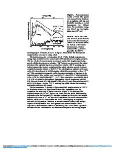
Abstract Photoluminescence (PL) measurements of thin rapidly annealed As implants have been made. The experimental conditions required to enhance the PL signal from the implant region have been established. Our data suggest that residual defects within the implanted volume can completely quench the PL signal.
For the range of anneal times investigated (0.3s to 10s) we find that temperatures above 1050"C are needed to remove these defects. Anneal temperatures of 1350"C remove the defects sufficiently to allow us to observe strong PL from the implanted volume..
Introduction Our aim in this work was to see how useful photoluminescence may be in detecting and characterising relatively thin As implants in silicon. Photoluminescence is a non-destructive contactless technique and measures electronic properties. This is an important point because, although analytical techniques like Secondary Ion Mass Spectrometry (SIMS) are invaluable for measuring atomic concentrations in thin heavily doped structures, the measurement of electrical properties of such systems is a difficult task. Transmission electron microscopy (TEM) analysis of the extended defect structure is also a difficult, time consuming task. Both TEM and SIMS require extensive sample processing. In a PL measurement we detect radiative recombination at dopant atoms, but the signal strength depends also on competition for the recombination traffic due to non-radiative processes at other defects in the solid. In heavily doped material Auger recombination may also play a role [11. In principle, however, PL is a technique which is sensitive both to dopant concentration and to electrically active defects.
Mat. Res. Soc. Syrup. Proc. Vol. 100. 91988 Materials Research Society
324
We find that recombination competition plays an important role in our ability to detect luminescence from the implanted dopant, and that impurities in the underlying wafer as well as defects in the implant region can control the form of the PL spectrum. The relative importance of these competative paths depend on the measurement temperature and the Adequately annealed samples can yield PL spectra which
degree of annealing of the wafer.
are dominated by the implanted dopant, provided the experimental conditions are correct.
Experimental Details Samples were boron doped (10-20 n cm) wafers, implanted at 5OKeV with an As The wafers were annealed with an Ar discharge lamp system. Set anneal times of 0.3, 2 and 10s were used; and for each anneal cycle two temperatures, 1050 and 1350"C were employed. dose of 2.1015cm-2.
Photoluminescence was excited using the 514nm line of an Ar laser.
Sp
Data Loading...


