Photoluminescence Characterisation of Ion Implanted CdTe
- PDF / 95,090 Bytes
- 6 Pages / 612 x 792 pts (letter) Page_size
- 60 Downloads / 321 Views
Photoluminescence Characterisation of Ion Implanted CdTe D. P. Halliday, M. D. G. Potter, D. S. Boyle and K. Durose University of Durham, Department of Physics, South Road, Durham, DH1 3LE, United Kingdom ABSTRACT We have ion implanted a series of dopants into single crystal CdTe. The influence of the impurities on the CdTe has been studied by low temperature photoluminescence spectroscopy. The impurities studied are: O, Cl, Cu, S, Na and Sb, and were selected because of their potential importance in thin film CdTe/CdS photovoltaic devices. Each impurity was implanted to give a smooth gaussian distribution in the first few microns of material with a doping density of 1×1015cm-3. Low temperature photoluminescence spectra were recorded from each sample and compared with an undoped sample. The PL features observed in each sample are discussed and the data is compared to an earlier photoluminescence study of thin film CdTe/CdS photovoltaic device structures. INTRODUCTION The two most important factors limiting conversion efficiency in CdTe/CdS devices are the influence of impurities and the influence of grain boundaries on carrier recombination losses in these structures. This work addresses the issue of impurities in these device structures. EXPERIMENTAL DETAILS Low temperature photoluminescence (PL) spectroscopy was performed on a series of ion beam implanted single crystal CdTe samples. The spectra were recorded at 10K using excitation from an Ar+ laser. Details of the PL measurement technique have been published previously [1]. The CdTe was provided by eV Products Inc. and Br2/methanol polished on the ( 111 )B face. Table 1 shows the dopant densities and accelerating voltages used to implant the impurities into the CdTe. Accelerating voltages were chosen to produce a smooth gaussian distribution of impurities in the first few microns of the material. Table 1 Accelerating voltages and doping profiles for implanted samples. Dopant Accelerating voltage (keV) Doping (cm-3)
Undoped N/A N/A
O 80 1x10¹⁵
Cl 80 1x10¹⁵
Cu 160 1x10¹⁵
S 160 2x10¹⁵
Na 80 1x10¹⁵
Sb 160 1x10¹⁵
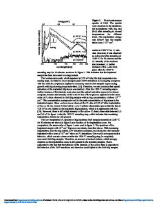
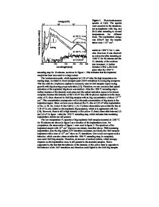
RESULTS & DISCUSSION The PL spectrum for the undoped sample is shown in figure 1. The features observed include a sharp near band edge emission at 1.590eV due to an acceptor bound exciton (A0X), with a weaker sideband to higher energies due to either donor bound exciton (D0X) or free exciton (FE) recombination. We are unable to resolve these very weak transitions at 10K. The peak at 1.576eV is a LO phonon replica of this weak exciton recombination shoulder at 1.6eV. A H1.8.1
PL Signal (Counts)
12000
Undoped
(A0X)
10000 (FE)-LO
8000
0
(A X)-LO
6000 4000
LO2
Y Y-LO1
2000
Y-LO2
0 1.40
1.45
(FE) or (D0X)
DAP 0 x100 eA LO1
1.50
1.55
1.60
Energy (eV) Figure 1 Low temperature (10K) PL spectra of undoped CdTe showing near band edge transitions as labelled on the diagram. The twin peaks around 1.525eV and 1.505eV are the LO1 and LO2 replicas of the eA0 and DAP transitions. LO phonon replica of the dominant near band edge A0X emission is
Data Loading...


