Characterization and Monitoring of Silicon-on-Insulator Fabrication Processes by High-Resolution X-ray Diffraction
- PDF / 288,525 Bytes
- 6 Pages / 612 x 792 pts (letter) Page_size
- 67 Downloads / 998 Views
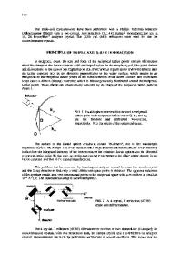
Characterization and monitoring of silicon-on-insulator fabrication processes by high-resolution x-ray diffraction G. M. Cohen, P.M. Mooney, H. Park, C. Cabral, Jr., and E.C. Jones IBM T. J. Watson Research Center, P.O. Box 218, Yorktown Heights, NY 10598, U.S.A Abstract High-resolution x-ray diffraction (HRXRD) was used to monitor silicon-on-insulator (SOI) processing steps. The use of HRXRD is attractive since it is non-destructive and can be applied directly to product wafers. We show the usefulness of this technique for the characterization of amorphizing implants for shallow junctions, solid phase re-crystallization of implanted junctions, cobalt-silicide formation, and oxidation; all are critical processes for CMOS fabrication on SOI. Introduction The idea behind the use of HRXRD to monitor SOI processing is straightforward. Oxidation, silicide formation and amorphizing implants reduce the single crystal SOI film thickness, which is easily and accurately measured by HRXRD [1]. For example, oxidation would convert the upper part of the SOI film into SiO2. Similarly, silicidation reacts a metal (such as Co) with the top portion of the SOI film to form a silicide (such as CoSi and CoSi2). The phase of the silicide that is formed can be determined from the amount of Si consumed. In the case of amorphizing implants, which are routinely used to form the source and drain region of a device [2], a portion of the SOI film is converted from single crystal silicon to amorphous silicon. Post-implant annealing, typically carried out by rapid thermal annealing (RTA), recrystallizes the amorphous portion of the film and restores the SOI film thickness. Accurate measurement of the SOI film thickness is essential for tight monitoring of all these processes. The change in the SOI layer thickness is not the only parameter obtained by HRXRD. The HRXRD data of amorphizing and non-amorphizing Ge, Si or boron implanted wafers, is further used to extract the strain profile and the implant damage profile in the SOI film. Moreover, in the case of boron-implanted wafers a change in the sign of the strain is recorded when the boron assumes a substitutional site following the RTA anneal. Experiment The x-ray diffraction measurements were carried out with a Philips materials research diffractometer (MRD), which is equipped with an asymmetrically cut four-crystal Ge(220) monochromator and mounted on a rotating Cu anode x-ray source. ω is the angle between the incident beam and the wafer surface and 2θ is the angle between the incident beam and the detector (reflected beam); therefore the angle of the incident or reflected beam with respect to the analyzed atomic planes, the Bragg angle, is θB = 2θ/2. φ denotes a rotation in the plane of the wafer. The 004 reflections were measured in the triple-axis (TA) mode [3], i.e. by taking ω/2θ scans with an analyzer crystal installed in front of the detector. The 113 reflections were measured using a large detector aperture and standard rocking curves (ω scans). The 113 reflections are taken with a l
Data Loading...