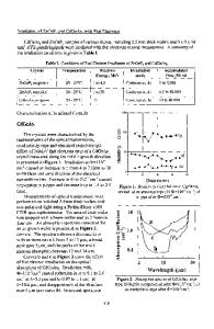
Characterization of CdGeAs 2 Using Capacitance Methods
- PDF / 295,143 Bytes
- 5 Pages / 414.72 x 648 pts Page_size
- 91 Downloads / 373 Views
S.R. SMITH*, A.O. EVWARAYE**, and M.C. OHMER Materials & Manufacturing Directorate, Air Force Research Laboratory, MLPO, WrightPatterson Air Force Base, OH 45377-7707 *University of Dayton Research Institute, 300 College Park, Dayton, OH 45469-0178 "**Universityof Dayton, Department of Physics, 300 College Park, Dayton, OH 45469-2314
ABSTRACT
Thermal Admittance Spectroscopy(TAS) has been used to detect energy levels in the bandgap of CdGeAs2 specimens. Capacitance-Voltage(CV) measurements were used to determine the net free carrier concentration of the specimens as well as the conductivity type. All specimens were found to be p-type. CV measurements determined that the free carrier densities ranged from 1.2 x 10" cm-3 to 8 x 1018 cm"3. Usually one peak (but in some cases two) was observed in the thermal admittance spectra. One peak present in two samples indicates an acceptor with a thermal activation energy of Ev+(0. 10-0.13) eV which corresponds closely to the value of 0.100.12 eV found from Hall effect measurements on these specimens. The additional peak observed could correspond to a second deeper acceptor at Ev+0.346 eV, however, the energy could not be accurately determined because the peak was not fully resolved. Evidence for the existence of two native acceptors from electron paramagnetic resonance has recently been reported which tends to support a two acceptor model.
INTRODUCTION
CdGeAs2 is a ternary chalcopyrite nonlinear optical material which is potentially useful for frequency conversion in the infrared because it has the largest nonlinear optical coefficient of any known phase-matchable compound (235 pm/V).1 It also has a wide transparency range (2.4-18 gm). The primary application of CdGeAs 2 is for frequency doubling the output of CO 2 lasers. Until recently large single crystals were not available; however, Schunemann has succeeded in overcoming the growth problems by using a seeded horizontal gradient-freeze growth technique with a temperature gradient of only a few degrees per centimeter and a very slow cooling rate.2 CdGeAs2 is a narrow band gap semiconductor. The generally accepted band gap value is 0.57 eV at room temperature.3 The band gap increases to 0.65 eV at 77 'K. 4 The principal source of charge carriers is acceptor-like defects. These acceptors are thought to originate primarily from native defects such as cation vacancies and cation disorder. These defects have been characterized by Hall effect5 and photoluminescence(PL), 6 by infrared absorption techniques, and by electron paramagnetic resonance(EPR).7 We have applied Thermal Admittance Spectroscopy (TAS) to determine the energies of shallow electronic levels. In addition, these measurements have yielded information about the band structure of the material. 581
Mat. Res. Soc. Symp. Proc. Vol. 484 © 1998 Materials Research Society
EXPERIMENTAL The technique of thermal admittance spectroscopy involves monitoring the response of a Schottky diode as a function of frequency and temperature. The details of this experiment have bee
Data Loading...


