Characterization of Defects in Silicon Ribbons By Combined Ebic and Hvem
- PDF / 1,227,792 Bytes
- 6 Pages / 417.6 x 639 pts Page_size
- 31 Downloads / 247 Views
297
CHARACTERIZATION OF DEFECTS IN SILICON RIBBONS BY COMBINED EBIC AND HVEM t
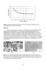
HORST STRUNK, BRIAN CUNNINGHAM AND DIETER AST Materials Science and Engineering, Cornell University, Bard Hall, Ithaca, New York 14853 ABSTRACT The electrical properties and crystallographic nature of linear and planar defects in EFG silicon ribbons were studied. A direct correlation between electrical and structural properties was obtained by imaging the same areas first with EBIC Coherent twin boundaries were found to be and then with HVEM. electrically inactive, but higher order twins and other grain boundaries generally enhanced minority carrier recombination. Partial dislocations confined to coherent twin boundaries were usually electrically active, but in certain instances partial dislocations were observed which had no apparent EBIC contrast. INTRODUCTION Rapid progress has recently been made in the production process of edge defined film-fed grown (EFG) silicon ribbon, a description of which can be found EFG ribbon is a promising material for the production of inexin ref. [1]. pensive solar cells and therefore an understanding of the relationship between the crystallographic nature of the defects and their electrical activity is desirable. This information can then hopefully be used to modify the ribbon growth process to reduce the density of electrically active defects which detract from solar cell efficiency. EFG ribbons typically contain a large number of linear boundaries, the majority of which is parallel to the growth direction. The electrical activity observed at these boundaries can vary greatly. Linear boundaries can be electrically active along their entire length, or show no detectable activity. A large number of boundaries show enhanced carrier recombination only along certain sections, resulting in a "dotted" appearance in EBIC. The differing electrical activity of these linear boundaries has previously been ascribed to the dislocation content of the boundaries [2] or to the amount of impurity In the present study two cases of decoration at boundary dislocations [3]. dotted EBIC contrast are considered. Although the EBIC appearance of both is similar it will be shown that the defects producing the effect are markedly different. EXPERIMENTAL The electrical properties of EFG silicon ribbons were investigated in the scanning electron microscope (SEM) operated in the electron-beam induced curSchottky diodes were produced by evaporating a thin film rent (EBIC) mode. (0500 X) of Al onto the surface. A high voltage electron microscope (HVEM) tOn leave from Max-Planck-Institut fUr Metallforschung, 7000 Stuttgart 80, West Germany.
Institut fUr Physik,
298 operating at an accelerating voltage of 1 MV was used to study the crystallographic nature of the defects in the ribbons. To correlate the electrical and structural properties of defects, areas were selected and mapped out in EBIC. Specimens 3 mm in diameter were then cut out from the ribbon and ion-milled from the back side until the EBIC mapped areas were contained in
Data Loading...