Characterization of Electrical Properties of Low Temperature GaAs
- PDF / 258,821 Bytes
- 6 Pages / 420.48 x 639 pts Page_size
- 113 Downloads / 429 Views
CHARACTERIZATION OF ELECTRICAL PROPERTIES OF LOW TEMPERATURE GaAs BIN WU, ASHISH VERMA, JOHN GAMELIN, HYUNCHUL SOHN%, SHYH WANG Department of Electrical Engineering and Computer Science, University of California, Berkeley, CA 94720. *Department of Material Science and Mineral Engineering, University of California, Berkeley, CA 94720.
ABSTRACT LT GaAs(220 0 C) was grown on an n+ substrate and capped with n+ GaAs grown at 600 0 C (n-i-n). Complete IV and CV measurements were performed. The IV characteristics exhibit ohmic, trap-filling and space-charge-limited regimes. We have developed a model based upon the compensation of background shallow acceptors by deep donor traps, large concentrations of which have been shown to exist in LT GaAs. Computer simulation of the IV curve is compared with experimental results. The "breakdown" is attributed to trapfilling under electron injection. It is also found that when the voltage across the structure is changed, the current takes several seconds to reach steady state. This is consistent with our model, which assumes slow trapping and detrapping in the LT GaAs. High frequency CV measurements show the capacitance to be fairly constant for voltages below "breakdown".
INTRODUCTION The epitaxial growth of GaAs on a GaAs substrate using molecular beam epitaxy (MBE) is generally conducted at substrate temperatures of approximately 600 0 C. It has recently been shown, however, that very good epitaxial surface morphology can be obtained using substrate temperatures below 300 0 C. Slightly conductive in its "as-grown" state, this low temperature (LT) GaAs has been found to become highly resistive upon annealing at temperatures of 500-600 0 C[l] . One very promising application for this material lies in the area of GaAs IC devices: it has been shown that the inclusion of an (annealed) LT buffer layer between the active region and substrate of a GaAs MESFET reduces the backgating effect, even in the presence of light[2]. In this paper, we report experimental electrical characteristics of LT GaAs and computer simulations which explain the observed electrical behavior of the samples.
Mat. Res. Soc. Symp. Proc. Vol. 241. @1992 Materials Research Society
46
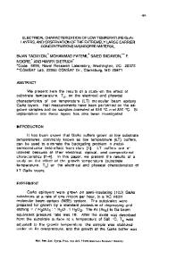
EXPERIMENTAL The test structure is shown in Fig.l. It is basically an n-in structure, where i denotes the LT region. AuGe/Ni/Au is used for ohmic contacts. Wet etching through the LT GaAs layer is used for 0 isolation. The n+ cap layer is grown at 600 C for 30 minutes, simultaneously annealing the LT GaAs. 100~300IrM
AuGe/Ni /Au
7-v7JM
n+ GaAs -----o0.
m
-- F
FIGURE 1. Experimental test structure.
n+ GaAs substrate AuGe/Ni/Au
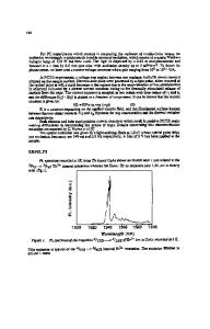
Shown in Fig. 2 is a typical i-v curve in log-log scale. The dotted line represents the experimental result. The curve, which is typical of SI GaAs, exhibits three distinct regions: ohmic, trap-filling, and space-charge-limited. The result is thus in agreement with other experiments which indicate a large density of deep traps in LT GaAs[3]. The results of the simulation, given by the solid line, will b
Data Loading...