Electrical Properties Of S + Implantation in Si GaAs
- PDF / 273,960 Bytes
- 5 Pages / 420.48 x 639 pts Page_size
- 97 Downloads / 360 Views
ELECTRICAL PROPERTIES OF S+ IMPLANTATION
IN SI GaAs
GUANQUN XIA, ANMIN GUAN, HAIYANG GENG AND WEIYUAN WANG Shanghai Institute of Metallurgy, Academia Sinica Shanghai 200050, China ABSTRACT The electrical properties of S+ implanted in SI GaAs have been studied. The rapid diffusion and redistribution of S+ implanted in GaAs after conventional thermal annealing (CTA) depends not on conventional diffusion of S+ or VAs, but on the enhanced diffusion by ion implantation. By employing rapid enhanced diffusion can be thermal annealing (RTA) techniques restrained, redistribution of S+ implantation can be decreased greatly and a thin active layer suitable for fabricating GaAs MESFET devices can be obtained. INTRODUCTION S+ implantation into Sl GaAs for n-type doping has been However, it can not be used for the frequently reported [1i. thin active layer in fabricating MESFET IC because of the carrier concentration redistribution caused by the rapid diffusion of S in GaAs during conventional thermal annealing (CTA). In this paper, S+ implantation in undoped SI GaAs has been studied. The doping behavior of S+ implanted in SI GaAs after CTA has been compared with that after rapid thermal annealing activation and carrier concentration (RTA). The electrical profile dependence on annealing temperature T, annealing time t and implantation dose 0 have been investigated. The reason for the redistribution of S+ implantation in GaAs has been discussed. EXPERIMENT The undoped SI GaAs substrates grown by LEC with crystal orientation of and resistivity p of 10 7 -10 8 Q.cm were used After chemical-mechanical polishing, the remainin this work. ing damaged layer was relieved by etching with 3H 2 SO 4 :lH 2 2 2:lH2 O The S+ was implanted at 7 off solution at 50°C for 5 min. 3 the crystal axis, energy 600 keV, dose between 2x10' 8x1014cm-2. The samples were annealed by capless As vapour CTA The implantation damage was analysed by Rutherand RTA (21. The activation efficiency, mobiliford backscattering (RBS). ty and carrier profile of implanted wafers were obtained by chemical C-V method. using Van der Pauw method and electrical The comparative experimental samples came from the same wafer. RESULTS Electrical activation and damaqe relief
of S + implantation
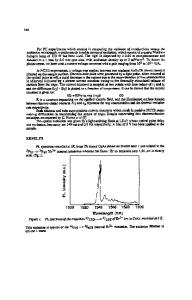
Fig.l shows sheet carrier concentration Ns as a function of dose 0 when S+ implanted in SI GaAs after annealing at 900 C for 15 min. It is observed that Ns becomes saturated and Mat. Res. Soc. Symp. Proc. Vol. 209. @1991 Materials Research Society
500
activation efficiency f reduced when >i014Ccm-2. And when Ns being saturated, 4 and n are superior to those given by references [3J. Table 1 lists data of average activation efficiency n and average mobility p of RTA and CTA samples. It shows that: (1) n increases with the increasing of CTA 0 temperature, while p increases at first and reduces at over 900 C. The optimal condition for CTA is at 900 Cfor 15 min. (2) n of RTA samples is higher than that of CTA. p of RTA samples is similar to that of CTA. Tab.
t
(s)
T (°C)
1
Comparison b
Data Loading...