Characterization of Graphene Gate Electrodes for Metal-Oxide-Semiconductor Devices
- PDF / 1,306,904 Bytes
- 6 Pages / 612 x 792 pts (letter) Page_size
- 74 Downloads / 425 Views
Characterization of Graphene Gate Electrodes for Metal-Oxide-Semiconductor Devices Yanbin An1, Aniruddh Shekhawat1,2, Ashkan Behnam3, Eric Pop3, and Ant Ural1 1
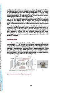
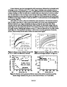
Department of Electrical and Computer Engineering, University of Florida, Gainesville, FL 32611 USA. 2 Department of Materials Science and Engineering, University of Florida, Gainesville, FL 32611 USA. 3 Department of Electrical and Computer Engineering, University of Illinois at UrbanaChampaign, Urbana, IL 61801 USA. ABSTRACT We fabricate and characterize metal-oxide-semiconductor (MOS) devices with graphene as the gate electrode, 5 or 10 nm thick silicon dioxide as the insulator, and silicon as the semiconductor substrate. We find that Fowler-Nordheim tunneling dominates the gate current for the 10 nm oxide device. We also study the temperature dependence of the tunneling current in these devices in the range 77 to 300 K and extract the effective tunneling barrier height as a function of temperature for the 10 nm oxide device. Furthermore, by performing high frequency capacitance-voltage measurements, we observe a local capacitance minimum under accumulation, particularly for the 5 nm oxide device. By fitting the data using numerical simulations based on the modified density of states of graphene in the presence of charged impurities, we show that this local minimum results from the quantum capacitance of graphene. These results provide important insights for the heterogeneous integration of graphene into conventional silicon technology. INTRODUCTION Graphene has attracted significant research interest for many applications in electronics, due to its excellent electrical conductivity, high optical transparency, mechanical flexibility, high thermal stability, and two-dimensional structure. However, the potential of graphene as a channel material replacing silicon is limited due to the absence of a bandgap. On the other hand, graphene is an excellent candidate as a transparent, conductive, and flexible electrode for siliconbased electronic and optoelectronic devices, including solar cells, gas sensors, and photodetectors. Unlike conventional metals, whose Fermi level is typically pinned at the surface, the Fermi level and hence workfunction of graphene can be tailored by electrostatic gating, chemical or contact doping, surface engineering, or by varying the number of graphene layers. As a result, graphene is also a promising candidate as a replacement for the gate electrode in metal-oxidesemiconductor (MOS) devices. In recent work, graphene has been used as the gate electrode of a nonvolatile charge-trap Flash memory device to replace TaN metal on top of a high- dielectric [1]. In another recent work, multi-layer graphene was incorporated between TiN metal gate and SiO2 in a MOS capacitor structure [2]. It was demonstrated that graphene electrodes improve the device performance in both cases. However, a detailed study of the electrical properties of graphene/SiO2/Si MOS structures is currently lacking. In particular, a study of the gate tunneling
Downloa
Data Loading...