Characterization of Structural Quality of Bonded Silicon-On-Insulator Wafers by Spectroscopic Ellipsometry and Raman Spe
- PDF / 113,036 Bytes
- 6 Pages / 612 x 792 pts (letter) Page_size
- 46 Downloads / 377 Views
B8.19.1
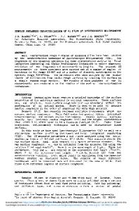
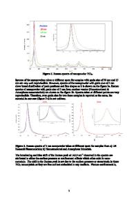
Characterization of Structural Quality of Bonded Silicon-On-Insulator Wafers by Spectroscopic Ellipsometry and Raman Spectroscopy N. V. Nguyen,a J. E. Maslar,b Jin-Yong Kim, a Jin-Ping Han,a Jin-Won Park,a D. ChandlerHorowitza , and E. M. Vogel a . a Semiconductor Electronics Division, bProcess Measurements Division, National Institute of Standards and Technology, Gaithersburg, Maryland 20899, USA ABSTRACT The crystalline quality of bonded Silicon-On-Insulator (SOI) wafers were examined by spectroscopic ellipsometry and Raman spectroscopy. Both techniques detect slight structural defects in the SOI layer. If a pure crystalline silicon dielectric function is assumed for the SOI layer, the spectroscopic ellipsometry data fitting yields an unacceptably large discrepancy between the experimental and modeled data. The best fits for all the samples result in a dielectric function of the SOI layer that consists of a physical mixture of crystalline silicon and about 4 % to 7 % of amorphous silicon. Using such a mixture indicates that there are still some defects in the SOI layer when compared with the high-quality bulk crystalline silicon. This observation is further supported by Raman spectroscopy measurements. The Raman spectra of all SOI samples exhibit a feature at about 495 cm-1 that is not observed in the crystalline silicon spectrum. Features similar to the 495 cm-1 feature have been reported in the literature and attributed to dislocations or faults in the silicon lattice. INTRODUCTION Bonded Silicon-On-Insulator (SOI) wafer developments are aimed at replacing bulk crystalline silicon (c-Si) substrates in mass production of CMOS and other advanced silicon devices because of the enhancement in speed and decreased power consumption possible with SOI substrates compared to traditional bulk silicon substrates. Current bonded wafer technologies [1] include SmartCut, NanoCleave, and ELTRAN.* As emphasized in the International Technology Roadmap for Semiconductors (ITRS) [2], structural and defect characterizations of SOI wafers are critical for understanding and improving the fabrication processes, and also advancing material metrologies. Major past studies by spectroscopic ellipsometry (SE) focused on SOI in earlier separation-by-implantation-by-oxygen (SIMOX) structures. It is only recently that bonded SOI wafers were examined by SE [3]. In this report, we combined SE and Raman spectroscopy to characterize a set of bonded SOI wafers fabricated by the SmartCut method. The results from both measurements show that residual crystal defects still exist in the SOI layer. The presence of residual defects is deduced because a *
Certain commercial equipment, instruments, or materials are identified in this paper in order to specify the experimental procedure adequately. Such identification is not intended to imply recommendation or endorsement by the National Institute of Standards and Technology, nor is it intended to imply that the materials or equipment identified are necessarily the best available for the purpo
Data Loading...