Controlled Synthesis of Si Nanopillar Arrays for Photovoltaic and Plasmonic Applications
- PDF / 278,288 Bytes
- 6 Pages / 432 x 648 pts Page_size
- 67 Downloads / 434 Views
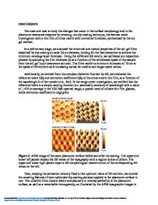
Controlled Synthesis of Si Nanopillar Arrays for Photovoltaic and Plasmonic Applications Umesh Gautam1, Jun Wang1, Dilip Dachhepati1, Seyyedsadegh Mottaghian1, Khadijeh Bayat2 and Mahdi Farrokh Baroughi1 1 Department of Electrical Engineering and Computer Science, South Dakota State University, Brookings, SD 57007 2 Harvard School of Engineering and Applied Sciences, 29 Oxford Street, Cambridge, MA 02138, USA ABSTRACT This paper focuses on developing a robust process to independently control the geometrical parameters of Si nano-pillar (NP) arrays. These parameters include height and diameter of NPs, spacing between them, and the shape of the NPs. We have shown that the diameter, height, and spacing of NPs can be independently engineered by controlling the diameter of nano-beads through synthesis procedure, duration of isotropic SiO2 etching and duration of anisotropic Si etching, respectively. INTRODUCTION Nanostructure arrays have shown strong potential for enhancing optical path length and light scattering in photovoltaics (PVs) and near field electromagnetic field enhancement for plasmonic applications [1]. Nano-pillar (NP) arrays have found promising applications in the fields of PVs and plasmonics. In the field of PVs, nanostructure have been utilized to 1) reduce reflection losses at the surface of solar cells and 2) break the trade-off between light absorption and charge collection by replacing vertical charge transport pathways with a radial path [2,3]. Independence of light absorption from charge separation in these solar cells enables them to achieve a reasonable PV performance even on very low quality, in terms of excess carrier lifetime, PV materials [4]. Significant progress has been made for development of methodologies for formation of Si NP in recent years [5]. Si NPs have been synthesized by chemical vapor deposition (CVD) via vapor-liquid-solid (VLS) growth technique. Kendrick et al. reported radial junction Si solar cells using Si wire arrays grown by Au catalyzed VLS growth on patterned Si substrates and achieved a power conversion efficiency of 2.3% [6].The remnants of metal atoms from the catalyst in the Si wires behaved as deep traps and seriously reduced the open circuit voltage of the device. Optical and electron beam lithography have been utilized for development of Si NP arrays [7] However, optical and electron beam lithography in deep sub-micron regime are expensive processes. Self-assembly of silica nano-beads followed by reactive ion etching of Si substrate using the self-assembled particles as the etching mask, has gained significant attention for development of Si NPs. This method, so called nano-sphere lithography, was utilized by E. Garnett et al. for development of vertically aligned Si NPs over a large area of 4x4 cm2 [1]. Successful utilization of this method in PVs and plasmonics require stringent control on the geometrical parameters of the NP array [4, 8-10]. For example, Paudel et al. showed that field enhancement in 2.5 dimensional plasmonic crystals is highly dependent on
Data Loading...