Arrays of Well-Defined Size-Tunable Metallic Nano-Cones for Plasmonic Applications
- PDF / 1,192,782 Bytes
- 4 Pages / 612 x 792 pts (letter) Page_size
- 103 Downloads / 346 Views
1055-GG10-04
Arrays of Well-Defined Size-Tunable Metallic Nano-Cones for Plasmonic Applications Monika Fleischer1, Florian Stade1, Andreas Heeren1, Michael Haeffner1, Dieter P. Kern1, Kai Braun2, Catrinel Stanciu2, and Alfred J. Meixner2 1 Institute of Applied Physics, University of Tuebingen, Auf der Morgenstelle 10, 72076 Tuebingen, Germany 2 Institute of Physical and Theoretical Chemistry, University of Tuebingen, Auf der Morgenstelle 8, 72076 Tuebingen, Germany
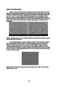
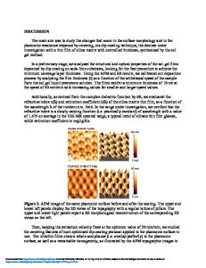
ABSTRACT Cones composed of noble metals with dimensions of the order of 100 nm, especially gold cones, are extremely well suited for optical near-field investigations using visible light. Their plasmon resonance frequency lies within the range of visible light frequencies, and upon illumination, strong electric field enhancement can be observed in the direct vicinity of the cone tip. For this purpose, a method to fabricate well-controlled nanocones with sharp tips is required. We present a top-down process in which arrays of cones are dry-etched from a metal stack on silicon. During the ion milling step, patterned hydrogen silsesquioxane resist is used as an etch mask. The resulting cones have tunable base diameters around 150 nm and tip radii down to less than 10 nm. Their optical characteristics are investigated by means of apertureless optical nearfield microscopy, in which field enhancement at the cone tip is observed. INTRODUCTION Obtaining localized regions of high electric field enhancement is one of the primary aims in the field of plasmonics. These are especially pronounced in the direct vicinity of metallic tips, where plasmons are generated within the metal upon laser irradiation. The local field enhancement can be utilized for applications like scanning near-field optical microscopy, Raman spectroscopy, optical antennas and optoelectronic devices, or lithography. The plasmon resonances depend strongly on the geometry of the metallic structures. To achieve pointed metallic nanostructures, tips have been prepared by focused ion beam techniques (e.g. [1]), by ebeam lithography and lift-off (e.g. [2]) or by adhering metallic colloidal nanospheres to nonmetallic tips (e.g. [3]). These methods often meet only one of the requirements of either sharp tips or reproducible structures at the nanometer scale. Therefore we developed a fabrication process for arrays of well-defined metallic nanocones [4] with tip radii of less than ten nanometers. The individual cones are excellent model systems for studying the interaction between light and metallic nanostructures. They can act as probes for scanning near-field optical microscopy, and two tips can be combined to form a vertical antenna structure [5]. Fabricating whole arrays of individual cones enables us to evaluate the reproducibility of the process and investigate the dependance of the field enhancement on small deviations in geometry. As a future application, one could also excite a whole array to obtain a grid of localized near-field probes for analyzing large-area samples.
FABRICATION The fabrica
Data Loading...