Controlling Environment and Contact Materials to Optimize Ohmic Microrelay Lifetimes
- PDF / 3,017,194 Bytes
- 6 Pages / 432 x 648 pts Page_size
- 27 Downloads / 390 Views
Controlling Environment and Contact Materials to Optimize Ohmic Microrelay Lifetimes Vitali Brand1, Michael S Baker2, Maarten P de Boer1 1 2
Mechanical Engineering, Carnegie Mellon University, Pittsburgh, PA 15213 USA. Sandia National Labs, Albuquerque, NM 87185 USA.
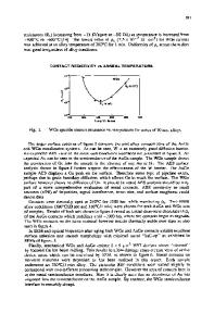
ABSTRACT There has been a recent resurgence in interest in developing ohmic switches to complement transistors in order to address challenges associated with electrical current leakage. A critical limitation in ohmic switches remains the reliability of their electrical contacts. These contacts are prone to hydrocarbon induced contamination which progressively inhibits signal transmission, eventually leading to device failure. We report on progress made towards controlling the contamination phenomenon. We discuss how contact materials and operating environment affect device performance, showing that RuO2 coated microswitch contacts operating in the presence of O2 experience very limited contaminant accumulation even in hydrocarbon-rich environments. We then demonstrate that devices which have experienced contamination can recover their original performance by being operated in clean N2:O2 environment. Finally, we suggest that this resistance recovery is associated with the chemical transformation of the contaminant as opposed to its removal and that the transformed contaminant may shield the Pt coating from oxidation. INTRODUCTION Ohmic switches have a wide range of applications where very low power consumption, low contact resistance, and excellent electrical isolation are critical [1]. On the microscale, these devices are already being implemented in applications such as RF communications [2, 3]. On the nanoscale there has been recent, broad interest of ohmic relay implementation in logic circuits [4, 5]. Today, Metal Oxide Semiconductor Field Effect Transistors (MOSFETs) are the fundamental component for logic computations. However, as linewidth shrinks below 100 nm, a critical shortcoming is their electrical leakage [4]. Complementing transistors with ohmic relays is an attractive approach because an air gap provides excellent electrical isolation. This approach also enables low power digital computation because the lowest voltage level at which siliconbased CMOS can operate is ~1 V, whereas an ohmic nanoswitch can operate at voltage below 0.1 V [6]. Considering that the energy per switch cycle is CV2 (C is capacitance), ohmic nanoswitches can operate with 100 to 10,000 times less energy per switching event than MOSFETs. These power savings would be ideal for electronics involving batteries and to reduce overheating issues. Despite the substantial advantages of ohmic switches, reliability of their electrical contacts remains a pressing concern for both micro- and nanoscale applications. The main challenge is associated with circuit failure due to high electrical contact resistance, Rc (effectively preventing signal transmission). Contact degradation mechanisms such as wear [7] and material transfer [8] are known contributing factors to high ܴ , th
Data Loading...