Transparent ZnO-Based Ohmic Contact to p-GaN
- PDF / 677,915 Bytes
- 6 Pages / 612 x 792 pts (letter) Page_size
- 28 Downloads / 347 Views
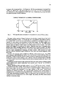
TRANSPARENT ZnO-BASED OHMIC CONTACT TO p-GaN E. Kaminska1, A. Piotrowska1, K. Golaszewska1, M. Guziewicz1, R. Kruszka1, A. Kudla1, T. Ochalski1, A. Barcz1,2, T. Dietl2, F. Matsukura2,3, M. Sawicki2, A. Wawro2, M. Zielinski2, J. Jasinski4, Z. Liliental-Weber4 1 Institute of Electron Technology, Al. Lotnikow 46, 02-668 Warsaw, Poland 2 Institute of Physics, PAS, Al. Lotnikow 46, 02-668 Warsaw, Poland 3 Research Institute of Electrical Communication, Tohuku University, Sendai 980-8577, Japan 4 Lawrence Berkeley National Laboratory, Berkeley, CA 94720, U.S.A. ABSTRACT Highly conductive ZnO films were fabricated on p-GaN in a two-step process. First, zinc was thermally evaporated on p-GaN. Next, zinc film was oxidized in oxygen flow. To increase the conductivity of ZnO, nitrogen was introduced into zinc during its deposition. The above procedure proved successful in fabricating ZnO of the resistivity of ~1x10⁻³Ωcm and resulted in ohmic contacts of resistivity ~1x10⁻²Ωcm2 to low-doped p-GaN, and light transmittance of ~75% in the wavelength range of 400-700 nm. INTRODUCTION In a variety of optoelectronic applications, such as light-emitting, -detecting and -triggered semiconductor devices the top electrode serves as both ohmic contact and optical window. For GaN-based photonic devices, where the major losses of performance are due to poor conductivity of p-type subcontact region, causing the so-called “current crowding” problem, a highly conductive and transparent p-type electrode is a prerequisite. Among the investigated metallizations that would allow low-resistivity contact to p-GaN, oxidized Ni/Au bilayer was reported to give the lowest operating voltages [1-3]. For the transparent p-type electrode, optimization of Ni/Au metallization via reducing its thickness [4,5] has been achieved, however, at the cost of increase of the specific contact resistance. Another approach for obtaining effective current-spreading layer, providing low-resistivity contact to p-type GaN in conjunction with efficient and uniform light emission, would be to make the p-type contact/window layer from a transparent conducting oxide (TCO). Following this approach, indium tin oxide (ITO) films have been recently tested as electrical contacts to p-side of GaN-based light emitting diode (LED), vertical cavity laser (VCSEL) and resonant cavity LED, allowing satisfactory lateral current spreading and required transparency [6,7]. Below, we report on the use of ZnO as an ohmic contact to p-GaN. This material is an excellent candidate for a thermally stable heterojunction contact to p-GaN. Both materials posses the same wurtzite structure with small lattice mismatch. As compared to ITO, ZnO offers higher chemical stability at higher temperatures [8, 9]. The transport properties of ZnO depend strongly upon the stoichiometry and on the nature and concentration of impurities and dopants introduced into the film [9]. Usually, ZnO films are fabricated by sputtering [10] or pulsed laser-deposition [8, 9]. New idea of this work is to form highly conductive ZnO
Data Loading...