Ohmic Contact Behavior of Pt/Ni/Au to p -ZnO
- PDF / 112,227 Bytes
- 6 Pages / 612 x 792 pts (letter) Page_size
- 56 Downloads / 396 Views
0928-GG09-12
Ohmic Contact Behavior of Pt/Ni/Au to p-ZnO Ji-Myon Lee1, Kyoung-Kook Kim2, Hitoshi Tampo2, Akimasa Yamada2, and Shigeru Niki2 1 Materials Science and Metallurgical Engineering, Sunchon National University, 315 Maegokdong, Sunchon, Chonnam, 540-742, Korea, Republic of 2 AIST, Tsukuba, Ibaraki, 305-8568, Japan
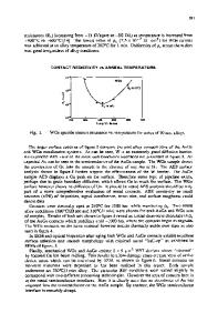
ABSTRACT The electrical properties of single Pt (30 nm) and Pt (30 nm)/Ni (30nm)/Au(50nm) multilayer contacts on moderately doped p-ZnO (Na = 5.0 × 10¹⁷ /cm3) were investigated. Although linear current-voltage characteristics were observed for all samples, a sample that was annealed for 1 min at a temperature above 500 oC resulted in an ohmic contact with good characteristics. The best ohmic contact to p-type ZnO was obtained using a Pt/Ni/Au multilayer contact that was annealed at 600 oC for 1 min under a N2 ambient, showing a specific contact resistance Rc of 1.97 × 10⁻⁵ Ωcm2. The fundamental mechanisms for the lower contact resistivity of Pt/Ni/Au contacts are discussed based on glancing angle x-ray diffraction results and Auger depth profile analysis of the multilayer alloying process. Furthermore, we fabricated a ZnO p-n homojunction using Pt/Ni/Au and Ti/Au as the p-type and n-type ohmic contact metal, respectively. The threshold voltage was determined to be about 3.7 V, comparable to the bandgap energy of ZnO. INTRODUCTION Zinc oxide (ZnO) is a promising II-VI compound semiconductor for applications in optical devices such as light emitting diodes (LEDs), laser diodes (LDs), and UV photodetectors, because of its high bond strength (cohesive energy of 1.89 eV and melting point of 2248 K), and the large exciton binding energy of 60 meV [1]. Along with the availability of a large-area substrate, low growth temperature, high radiation resistance, and relatively low material costs [2,3], the fabrication of high quality multi-quantum well, by alloying with MgO, has been achieved, which opens the possibility of the development of efficient optoelectronic devices from ZnO films [3]. Very recently, electroluminescence spectra from the p-n and p-i-n junction has been reported, by exploiting p-type ZnO films that has been doped with phosphorous by magnetron sputtering and nitrogen by laser molecular beam epitaxy [4,5]. Thus, the development of optoelectronic devices from ZnO films has become a reality. Currently, attention has been focused on enhancing the luminescence efficiency of optoelectronic devices via the use of ZnO materials, by analogy with the group III-nitride-based devices. Therefore, the development of a low resistance ohmic contact on ZnO is needed, since the major loss in device performance is frequently due to high resistance metal-semiconductor ohmic contacts [6], resulting in poor performance and device reliability [7]. While numerous data related to an ohmic contact to n-ZnO have been reported to date [8,9], only a few reports can be found in the literature on ohmic contact to p-type ZnO films [10,11].
In this paper, the ohmic characteristics of a Pt/Ni/Au multilayer to p-type Z
Data Loading...