Crystal Structure and Defects in Nitrogen-Deficient GaN
- PDF / 248,855 Bytes
- 6 Pages / 612 x 792 pts (letter) Page_size
- 93 Downloads / 287 Views
1 Downloaded from https://www.cambridge.org/core. IP address: 5.101.222.113, on 15 Sep 2019 at 13:55:27, subject to the Cambridge Core terms of use, available at https://www.cambridge.org/core/terms. https://doi.org/10.1557/S109257830000329X
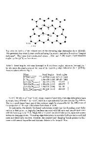
molecules which reduces atomic nitrogen concentration. Therefore, special efforts should be made to increase nitrogen incorporation into the growing layer. In the conventional processing methods for III-N growth, MOCVD and MBE, the special means for atomic nitrogen generation are utilized, such as high-temperature pyrolisis of ammonia in MOCVD, or plasma nitrogen sources in MBE. In the case of laser ablation, it is in principle possible to transfer the composition from the stoichiometric target to the substrate. In general, raising the growth temperature is effective in improving the crystallinity and purity of epitaxial films unless it causes thermal decomposition of the crystal, which occur in GaN above 600 0C. Therefore, it is important to determine the growth temperature range in which thermal decomposition does not limit the properties of the nitrides. In this letter, we will focus on structural properties of GaN films grown by MOCVD and PLD under nitrogen-deficient conditions. Experimental Details To study the influence of the stoichiometry on the film microstructure we used GaN films grown by MOCVD or pulsed laser deposition (PLD). These methods have very different thermodynamic and kinetic parameters, and, therefore, comparison of the results is crucial for both studying growth-property correlations as well as understanding the mechanisms of defect formation under nonstoichiometric conditions. Atmospheric pressure vertical MOCVD reactor with a mixture of trimethylgallium, ammonia and nitrogen as a carrier gas was used to grow GaN films on α-Al2O3 (0001) substrates. The details of growth can be found elsewhere [7]. The growth process included nitridation, growth of a low-temperature AlN buffer layers and GaN films. The latter films were deposited at 950 0C with an average V/III mole ratio of 1000. We have also employed PLD to grow GaN on α-Al2O3 (0001). We used KrF excimer laser (wavelength - 248 nm, pulse frequency - 10-15 Hz, pulse duration 20 ns) to ablate a stoichiometric hot-pressed target. Target-substrate distance of 4.5 cm, energy density of 3-4 J/cm2 were used to prepare 150-250 nm - thick films. The films were deposited at a substrate temperature of 720-800 0C in a vacuum chamber with a base pressure of 5x10⁻⁷ Torr on solvent cleaned substrates. The details of the target and substrate preparation, their characteristics and parameters of PLD are summarized elsewhere [8]. It should be emphasized that the PLD GaN films are much thinner (0.5 µm).. The characterization of defects and interfaces in the films was carried out using transmission electron microscopy (TEM). A 200 keV Topcon 002B microscope with a point-to-point resolution of 1.8 Å was used for this study. The cross-sectional TEM samples were prepared by mechanical polishing followed by dimpling to a thi
Data Loading...