Current Status of SiC Power Switching Devices: Diodes & GTOs
- PDF / 3,122,698 Bytes
- 10 Pages / 417.6 x 639 pts Page_size
- 67 Downloads / 526 Views
to be followed by demonstration of scaled up devices. While applications of devices with voltage ratings > 9 kV currently appears to be the realm of SiC devices, lower voltage applications face Table 1 Potential markets for SiC devices (in order of relative size) Typical device
Application area Motor controllers for Electric Vehicles Engine and airflow controls for aviation electronics
Schottky diode, MOSFET Schottky diode, MOSFET, sensors
Electric Utility Power applications
P-I-N diode, Thyristors
Industrial High voltage power electronics
P-I-N diode, MOSFET/IGBT
Ballasts for flourescent lamps
MOSFET
Conventional ICE automobile sensors/electronics
Sensors
HDTV transmitters
SIT
Surveillance and tactical radars
MESFET, SIT
23 Mat. Res. Soc. Symp. Proc. Vol. 572 © 1999 Materials Research Society
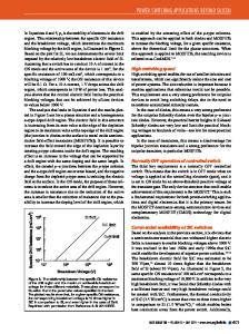
significant challenges from the concurrent development of alternative technologies. The expected improvement of silicon technology, illustrated by developments in silicon IGBT and MOSFFT devices, as well as interest in other materials for power device applications 3 are cases in point of the need for timely identification and resolution of outstanding technical issues to obtain continued performance and reliability improvements of SiC power devices. This paper focuses only on issues related to the development of SiC diodes and thyristors. Material quality Material quality is an important issue for the fabrication of high power devices. Much of the research being performed on high voltage devices are presently aimed at devices having ratings of at least 1-10 A/-I kV, increasing to 100-1000A/5 kV. The need to minimize on-state voltages 2
limits practical devices to current densities of - 500 to 1000 A/cm . Such a rating is sufficient to
enable conductivity modulation, without significant carrier-carrier and Auger scattering induced 2 resistance and will require device sizes between 5 and 20 mmi. However, present devices are limited by catastrophic voltage degradation due to hollow-core screw dislocation ("micropipe") bulk defects which exist in densities of as low as 30 cm-2 . Thus, device size is limited to -1 mm 2 . Progress in this area is incremental. Because, it is well known that the distribution is NOT uniform one approach to device scaling has been to selectively place devices in sufficiently large micropipe-free areas of the wafer. This approach neglects the contribution of other defects. Another approach would be to parallel many smaller devices. While possible for unipolar device,., the success of this strategy will have to be demonstrated for bipolar devices since current hogging in the on-state and uniform switching to prevent catastrophic destruction are potential problems, especially forGTOs. Fig. 1 shows the breakdown voltage of devices of various sizes. It is clear from the figure that devices much smaller than 1 mm 2 have severely degraded breakdown characteristics. The 3 observed degradation is consistent not with micropipe defects, but rather with - 10 to 10 cm-2 defect densities associate
Data Loading...