Microprobe Raman Analysis of Picosecond Laser Annealing of Implanted Silicon
- PDF / 1,040,539 Bytes
- 6 Pages / 417.6 x 639 pts Page_size
- 59 Downloads / 396 Views
MICROPROBE RAMAN ANALYSIS OF PICOSECOND LASER ANNEALING OF IMPLANTED SILICON
J. SAPRIEL, Y.I. NISSIM and J.L. OUDAR Centre National d'Etudes des T6lcommunications*, BAGNEUX - (FRANCE)
196 rue de Paris 92220
ABSTRACT Picosecond laser annealing has been performed on implantationamorphised silicon. A multiannular (up to five rings) recrystallization pattern has been generated by a single"30 psec pulse at 1.06 pM and 0.53 pm wavelength and energy density just below the damage threshold. The different patterns have been investigated by scanning the surface with a Raman microprobe with a 1pm spacial resolution. Information are thus given on the different phases (amorphous or crystalline) and on lateral as well as in depth dimensions of the different rings.
INTRODUCTION The study of picosecond laser annealing of implanted silicon and the use of Raman scattering as a versatile and non destructive tool for the characterization of the recrystallization pattern is reported here. A rather complete set of experiments are presented on silicon samples, at different annealing enersingle pulse annealing is gies and wavelengths. Each pattern resulting from analysed parallel and perpendicular to the free surface. When a pulsed beam is used to anneal implanted silicon, it is likely that liquid melting of a surface layer occurs during irradiation, followed by phase epitaxial regrowth. The resolidification time is of the order of tens of nanoseconds. The velocity of the solid-liquid interface is thus slow enough for the lattice to reconstruct. However disordered material can be formed when this velocity is increased above the value necessary for epitaxial regrowth to take in single crystal silicon for place. Such high resolidification rates occur extremely high absorption (U.V. photons in the nanosecond regime [1]) or with extremely short pulses (picosecond irradiation [2])resulting in amorphous silicon formation. On ion implanted amorphized silicon similar experiments led to an annular recrystallization pattern [3,4] formed with single crystal, amorphous and polycrystalline materials. SAMPLE PREPARATION AND TRE PICOSECOND ANNEALING Single crystal silicon (100) oriented, were implanted with As+ ions at a 2 5 and at an energy of 100 keV creating A 1000 A thick amordose of IxlO1 /cm phous layer. The annealing was carried out with a mode locked Nd-YAG laser described in ref [5]. Single pulses of average duration 27 psec at 1.06pm and 20 psec at 0.53 pm can be extracted from this system. The sample was placed at * Laboratoire associ6 au CNRS (LA250)
Hat.
Res.
Soc. Symp.
Proc. Vol.
13
(1983) Q Elsevier
Science Publishing Co.,
Inc.
236
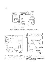
the focal point of a one meter focal length lens. The laser was operated at a low repetition rate in combination with a shutter, so that the sample could be translated between each pulse. Each pulse focused through the lens had a gaussien spatial and temporal profile. The spatial profile is visualized on an array of photodiodes in Fig.l.
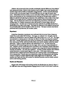
Mamorphous region 0
single crystal
the pi distribution o
Data Loading...