Damage Production in B-Sic During Ion Implantation
- PDF / 1,437,742 Bytes
- 6 Pages / 417.6 x 639 pts Page_size
- 48 Downloads / 378 Views
DAMAGE PRODUCTION IN B-SiC DURING ION IMPLANTATION S. P. WITHROW,* K. MORE,*** JOHN A. EDMOND,** H. S. KONG** P. J. MAZIASZ* AND R. F. DAVIS* *Oak Ridge National Laboratory, Oak Ridge, TN 37831 ***Oak Ridge Associated Universities, Oak Ridge, TN 37831 "**Department of Materials Engineering, North Carolina State University, Box 7907, Raleigh, NC 27695-7907
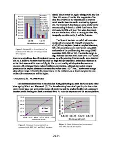
ABSTRACT Damage in single crystal B-SiC(100) as a result of ion bombardment has been studied using Rutherford backscattering (RBS) and cross-section transmission electron microscopy (X-TEM). Samples were implanted with 123 keV 2 7 AI at liquid nitrogen temperature. RBS spectra for He channeling in the (110) axis at 450 were obtained as a function of implantation dose to determine damage accumulation. X-TEM was used to characterize damage structure for selected doses. The surface of the SiC becomes amorphous for doses greater than 1 x 10¹⁵ /cm 2 . At lower doses, significant uniaxial lattice strain along the (100) direction is suggested by comparison of RBS channeling spectra obtained for several high index axes. High resolution TEM on a sample implanted at 4 x 10¹⁴ /cm 2 shows no damage structure in the surface region; lattice damage in a broad layer centered roughly at the depth of highest energy deposition is characterized by small amorphous pockets in a crystalline matrix. Qualitatively similar backscattering results were obtained for other elements implanted at room and liquid nitrogen temperature.
INTRODUCTION Ion implantation has recently been used as a method of dopant introduction into B-SiC.[lJ] As with other semiconductors, doses in the range 1013 to 1015 /cm 2 are sufficient to create considerable damage in the lattice. Eventual amorphization of the structure occurs. While the production of disorder and amorphization via implantation has been studied in some semiconductors[2] as well as other polymorphs of SiC[31, little work has been reported on the nature of the damage occurring in B-SiC, a candidate material for high temperature semiconductor devices. The precise disorder structures produced by ion implantation into semiconductors are complicated. In the present work, Rutherford backscattering (RBS) in a channeling geometry has been used to determine the depth and amount of damage accumulation as a function of dose for Al ion implantation into B-SiC at liquid nitrogen temperature. Cross section transmission electron microscopy (X-TEM) has been used to characterize the microscopic nature of the defects present in the doped material. This work is part of an ongoing study of electronic device production in B-SiC.[1,4]
Mat. Res. Soc. Symp. Proc. Vol. 74. c 1987 Materials Research Society
374
EXPERIMENT AND RESULTS Thin films (up to 15g) of single crystal B-SiC were epitaxially grown on (100) silicon wafers via chemical vapor deposition.[5] After mechanical polishing and 27 A1 at etching, the samples were implanted at liquid nitrogen temperature with 123 keV. Accumulation of damage in the crystal lattice was characterized by RBS spectra obtained in
Data Loading...