Stoichiometric Disturbance in InP Measured During Ion Implantation Process
- PDF / 999,673 Bytes
- 5 Pages / 417.6 x 639 pts Page_size
- 31 Downloads / 314 Views
STOICHIOMETRIC DISTURBANCE IN InP MEASURED DURING ION IMPLANTATION PROCESS D. HABERLAND, P. HARDE, H. NELKOWSKI Technical University Berlin, D-1O00 Berlin 12, West-Germany and W. SCHLAAK Heinrich-Hertz-Institut,
D-1O00 Berlin 12, West-Germany
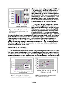
ABSTRACT To measure the sputtered ions during implantation a specially designed UHV-target chamber with a SIMS apparatus was set up. Quantitative analysis are possible with an Auger spectrometer. Disturbances in the stoichiometry in InP are measured during implantation of Sn. The enrichment of the doped surface of InP with the lighter component phoshorus will be discussed in consideration of preferential sputtering and recoil effects during implantation. Measured depth profiles of Sn in InP will be compared with calculated distributions on condition that sputtering takes place. The sputtering yield of InP bombarded by 120 keV Sn+ is 17+5. INTRODUCTION With the growing interest of the electronic industry in III-V compound semiconductors the use of ion implantation to dope such materials has become quite important in the last few years. Indium phosphide and its ternary and quaternary compounds are used to manufacture electro-optical and electronic devices. As in silicon technology the advantages of ion implantation include the good control over carrier concentration, uniformity, and reproducibility. However, apart from radiation damage new problems arise in compound semiconductors. Preferential sputtering and recoil effects will lead to stoichiometric disturbances in the implanted layer (1). These effects could influence the electrical activation of dopants, or in case of amphoteric dopants, changes the probability of occupancy of the suitable lattice sites. Particularly for InP we expect these disturbances because of the large difference in masses of the components. In this paper we will report on the decomposition of the doped surface of InP during implantation and present calculations which include the sputtering of the surface during implantation and explain quite successful the depth profile of secondary ion mass spectroscopy measurements. EXPERIMENTAL The reported measurements were carried out in a specially designed UHV surface analysis chamber connected to an implantation plant (2). This system makes it possible to observe sputter effects during implantation with almost any element at energies up to 170 keV. Figure 1 shows a schematic drawing of the surface analysis chamber. It consists of a SIMS system with an ion source, a quadrupole mass analyzer and an AES system (CMA with an integral electron gun) for quantitative surface analysis. A differential pumping stack with built-in deflecting plates connects the implaniation system to the UHV target chamber, so a pressure is maintained at 100-10 -l Pa during implantation. The quadrupole is mounted 900 to the implantation beam and to the beam of the SIMS ion gun. Thus it was achieved that measurements
Mat. Rs. Soc. Symp. Proc. Vol. 27 (1984)(Elsevier Science Publishing Co., Inc.
372
bea
FIG. 1: Schematic drawing of th
Data Loading...