A Reversible Effect of Rapid Thermal Annealing of Indium in Ion Implanted Silicon
- PDF / 355,469 Bytes
- 5 Pages / 414.72 x 648 pts Page_size
- 98 Downloads / 364 Views
35 Mat. Res. Soc. Symp. Proc. Vol. 470 01997 Materials Research Society
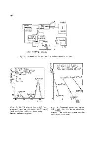
Fig. 1. RTA system with W-halogen 10 kW lamp. EXPERIMENT A W-halogen lamp was used in this experiment. The annealing was done at 1 atm. air pressure. A schematic of the RTA system used is shown in Fig. 1. The walls of the RTA system were made from a high reflective ceramic. The applied electrical power was 10 kW for all pulses. The distance between the -1mm thick quartz bulb and the sample was 1cm. The sample was mounted on a 3 point support. Two of these points were ceramic needles and the third was a thermocouple. The temperature of the sample was dictated by the duration of the pulse. The dependence of the sample temperature on the exposure time of a pulse for different exposures is shown in Fig. 2. 1200 1000 C.) jD
H•
800 600 400 200 0
15 10 Time, sec Fig. 2. The dependence of the sample temperature on the RTA pulse exposure time. 0
5
The maximum temperature of the sample for different pulse exposures is shown in Table I.
336
Table I. Maximum temperature of the sample as a function of the pulse time. Pulse time (sec)
Temperature(°C)
2
2.5
3
3.5
4
4.5
5
5.5
6
6.5
440 510 630 700 770 840 860 890 930 970
7
8
9.5
995
1010
1020
Phosphorus doped Silicon 380 gm thick wafers with 20 Ohm-cm resistivity were used 12 5 in this experiment. The samples were implanted with 1 In+ ions with a dose D=9.1 x10 2 cm- and 300 keV energy. The sheet resistance was measured by the four point probe method with a weight of 50g on the probe. The sheet resistance of unimplanted samples was 525 Ohm/sq. RTA process was performed on two different positions of the implanted side of the wafer relative to the source of irradiation (Fig. 3).
"* On the "front side facing" RTA, the doped side of the wafer was irradiated with the full spectrum of the incident light.
"• At the "back side facing" only transmitted light through the 380 jtm thick Si with X> 1.12 jgm reached the In doped layer of a sample. RESULTS After annealing on the "front side facing" position, the sheet resistance was reduced (pulses 3-7, 10-30, 32-33), see Fig. 4. The subsequent treatment following, on the "back side facing", resulted in an increase in the sheet resistance. The change in the annealing position from the "back side facing" to the "front side facing" is accompanied with a reduction of the sheet resistance of the doped layer (pulses 3,10,32). The reduction of the
sheet resistance was obtained in both cases: pulse 3 had an elevated temperature and pulses Light Light Doped side
(a)
(b)
Fig. 3. Two sample positions during the RTA annealing: (a) "front side facing", (b) "back side facing". 10 and 32 were at a lower temperature. The effect of In activation and deactivation existed after thirty of RTA pulses. It was reproducible on samples implanted with different energies of In+ ions: 40, 80 and 120 keV.
337
EXPOSURE OF RTA PULSE (sec.) ILiIn tO I n tn V) %D %D %Do N. OD%0%O q NqNqN04q M'M~MM'MV ~V V) D %0o Ir-C UsVO
%
5
(Y
U
4
Front side irradiation side irra
Data Loading...