Defect Densities and Carrier Lifetimes in Oxygen doped Nanocrystalline Si
- PDF / 223,852 Bytes
- 5 Pages / 432 x 648 pts Page_size
- 45 Downloads / 348 Views
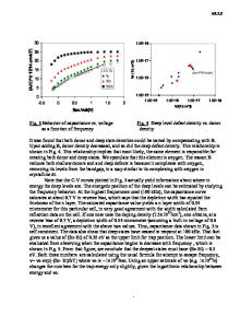
Defect Densities and Carrier Lifetimes in Oxygen doped Nanocrystalline Si Shantan Kajjam1, Siva Konduri1, Max Noack2 , G. Shamshimov3, N. Ussembayev3 and Vikram Dalal1 1 Department of Electrical & Computer Engineering, Iowa State University, Ames IA 50014 2 Microelectronics Research Center, Iowa State University, Ames IA 50014 3 Nazarbayev University, Astana, Kazakhstan ABSTRACT We report on the measurement of defect densities and minority carrier lifetimes in nanocrystalline Si samples contaminated with controlled amounts of oxygen. Two different measurement techniques, a capacitance-frequency (CF) and high temperature capacitancevoltage techniques were used. CF measurement is found to yield noisy defect profiles that could lead to inconclusive results. In this paper, we show an innovative technique to remove the noise and obtain clean data using wavelet transforms. This helps us discover that oxygen is creating both shallow and deep/midgap defect states in lieu with crystalline silicon. Minority carrier lifetime measured using reverse recovery techniques shows excellent inverse correlation between deep defects and minority carrier lifetimes through which hole capture cross section can be evaluated. INTRODUCTION Nanocrystalline Silicon (nc-Si) is an important material for solar cells and thin film transistors [1]. Its fabrication using plasma enhanced chemical vapor deposition (PECVD) is highly popular. Due to its method of fabrication, oxygen becomes a non-ignorable impurity and hence is important to study its degrading effects on device parameters. T. Kilper et al [2] have discussed about reduction in quantum efficiency due to presence of oxygen in the material that was introduced as a chamber leak. P. Hugger et al [3] showed variation in defect density versus oxygen content in the material. There is no previous study to indicate how the profile of defects varies within the band gap of nc-Si. We introduce oxygen systematically into the material and study the variation in defect densities, defect profiles and lifetimes. We also discuss the problem associated with measurement of defect profiles and provide a solution by using wavelet transform techniques and Matlab [4]. EXPERIMENT Nc-Si solar cells have been fabricated using very high frequency PECVD (45MHz) on stainless steel substrates. An n-i-p stack is made on the substrate with a-Si n+ and a thin nc-Si p+ at the top. The i-layer is made using hydrogen profile technique with silane and hydrogen at high dilution to attain an optimum crystallinity and a thickness of ~1.3-1.5μm. Controlled oxygen doping is done by using a 108ppm O2/He cylinder. Device contacts are ITO and sample is mesa-etched to reduce capacitance fringing. By covering ITO dots with wax and reacting the device with HF and HNO3, we can remove the non-waxed area of the device, thus leaving only
169
the dotted lined structure below the ITO contact in figure 1, and thereby reduce the influence of fringing fields on capacitance.
Figure 1. Schematic of the device Measurement Techniques Capacitance
Data Loading...