Density modulated nanoporous tungsten thin films and their nanomechanical properties
- PDF / 716,544 Bytes
- 14 Pages / 584.957 x 782.986 pts Page_size
- 91 Downloads / 346 Views
Muhammed T. Demirkanb) Department of Physics & Astronomy, University of Arkansas at Little Rock, Little Rock, AR 72204, USA
Kathleen A. Walsh Frederick Seitz Materials Research Laboratory, University of Illinois at Urbana-Champaign, Urbana, IL 61820, USA
Tansel Karabacak Department of Physics & Astronomy, University of Arkansas at Little Rock, Little Rock, AR 72204, USA
Andreas A. Polycarpoua) Department of Mechanical Engineering, Texas A&M University, College Station, TX 77843, USA (Received 30 December 2015; accepted 2 May 2016)
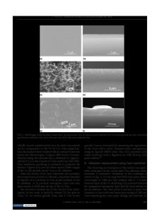
Density modulated tungsten (W) thin films with nanoscale porosity contents of 7% to 40% by volume were grown on Si substrates through magnetron sputter deposition. Process parameters were selected according to the structure zone model, which resulted in film thicknesses between 105 nm and 520 nm. Nanomechanical properties of samples were investigated by means of instrumented nanoindentation. Reduced-v2 analysis was carried out to assess four models formulated through differential effective medium approach. The model that factored in both the crowding effect and the maximum random packing of pores successfully captured the experimental trends. Attempts to breach the auxetic barrier resulted in large-scale pulverization or spontaneous conversion into WO3. Porosity corrected yield strength calculations underlined the possibility of defining a porosity threshold beyond which the compressive yield strength of density modulated nanoporous metallic thin films would drop abruptly due to aggravated geometric slenderness effects in agreement with earlier hypotheses.
I. INTRODUCTION
Tungsten (W) thin films possess significant technological potential in several applications such as x-ray masks and mirrors, photonic crystals, field emitters, and MEMS devices due to their inherent properties and functional capabilities highly sought in a multitude of fields ranging from solid state physics to nuclear engineering.1 Sputter deposition is a favorable method for thin films due to its low cost, easy implementation, and scalability in industry. However, problems such as, fragmentation or delamination encountered in submicron thickness regimes limit effective implementation in applications necessitating high quality thin films and coatings. During the growth of sputter deposited thin films, intrinsic stress emerges as one of the main causes for the delamination or
Contributing Editor: Yang-T. Cheng a) Address all correspondence to this author. e-mail: [email protected] b) Present address: Materials Science and Engineering Department, Gebze Technical University, Kocaeli, 41400, Turkey. DOI: 10.1557/jmr.2016.197
buckling depending on several deposition parameters such as substrate temperature and working gas pressure. Structure zone model (SZM) for sputtered thin films has been currently considered as the most successful model to analyze those parameters.2,3 The dependence of film microstructure and intrinsic stress on deposition parameters have been explored systematically by several research groups in the followi
Data Loading...


