Deposition and Characterization of Ultra-Thin Ta 2 O 5 Layers Deposited on Silicon from A Ta(OC 2 H 5 ) 5 Precursor
- PDF / 2,060,007 Bytes
- 6 Pages / 414 x 635.4 pts Page_size
- 77 Downloads / 324 Views
to maximize the film storage efficiency. In this work, we have studied the physico-chemical and electrical properties of ultra-thin Ta 20 5 layers deposited on nitrided Si substrates and annealed under different ambients.
EXPERIMENTAL DETAILS
Tantalum pentoxide thin films of three different targeted thicknesses (6, 8 and 10 nm) were fabricated on 8-inch. p-type Si(100) wafers (substrate doping _106 cm 3). As the first step, the silicon substrates were subjected to a rapid thermal nitridation (RTN) treatment in NH 3 at 850'C. The thickness of the resulting Si3N4 film is close to 1.2 nm (measured by ellipsometry). Ta 20 5 was deposited by low pressure chemical vapor deposition (LPCVD) at 450'C from an organometallic precursor, i.e.,
Ta(OC 2H5 )5. Samples were then annealed by employing three different treatments: 1) UV-0 3 at 445 0C for 2 min, 2) dry 02 at 750'C for 20 mrin, and 3) UV-0 3 at 445°C for 2 min followed by dry 02 at 750'C
for 20 min. Finally, aluminum dots of different areas were formed (by evaporation, photolithography
and etching) onto the Ta20 5 surface for electrical characterization. Since the crystallization temperature of tantalum pentoxide is close to 650°C, all the Ta 20 5 films annealed in 02 in this work were crystalline. The thicknesses of the various stacked structures were determined by ellipsometry with a fixed refractive index equal to 2.16. The physico-chemical characteristics were studied by transmission electron microscopy (TEM) and secondary ion mass spectroscopy (SIMS). The electrical properties were obtained from a computer-controlled HP4280A and HP4140B combined setup for high frequency capacitance-voltage (C-V) and current-voltage (I-V) measurements and for the study of the timedependent dielectric breakdown (TDDB) stress time dependence of cumulative failure of our capacitors. PHYSICO-CHEMICAL CHARACTERIZATION
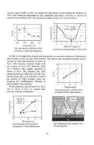
Ellipsometry measurements The thickness and uniformity of each structure studied in this work are presented in Fig. 1. The uniformity is below 2.3% for the three thicknesses and is more constant for as-deposited samples than for annealed samples. Concerning the thickness, it is clear from this figure that each annealing step leads to an increase of the thickness of the stacked structure. This suggests a growth of the interfacial film by means of an oxidation of the silicon substrate or of the nitride layer during the UV-0 3 and 02 post-
deposition annealing treatments. TEM measurements
To confirm this growth with 02 annealing, the interfacial region was studied by TEM. Results are shown in Fig. 2 in the case of a targeted thickness of Ta20 5 equal to 6 nm (as-deposited and UV-0 3 annealed layers). The thickness of the Si 3N4 layer is not affected by the deposition of Ta20 5 (Fig. 2(a)). 2--. _ 12 10
10
as-deposited
UV-O 3 annealed UV-O 3 + 02 annealed ,tut, 1r 02annealed 0
V-03 annealed 0- annealed 0
7
UV.0 3 +
2.0
2annealed
.6 U
4
C
2 6
6 8
8
Targeted thickness (nm)
10
Targeted thickness (nm)
Fig. 1: thickness and uniformity of each dielectric sta
Data Loading...