Characterization of Ta 2 O 5 Thin Films with Small Current Leakage for High Density Drams
- PDF / 3,338,747 Bytes
- 6 Pages / 415.8 x 637.2 pts Page_size
- 101 Downloads / 376 Views
Mat. Res. Soc. Symp. Proc. Vol. 592 ©2000 Materials Research Society
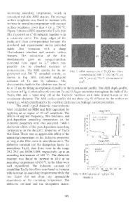
it in PH 3 . Amorphous Ta2O 5 films with a thickness of between 5 and 23nm were deposited on polysilicon by LP-CVD using tantalum penta-ethoxied (Ta(OC 2H5),) and oxygen. The amorphous Ta2O 5 film was then crystallized by rapid thermal oxidation (RTO). Before depositing Ta2 0 5 thin film, polysilicon was treated by rapid thermal nitridation (RTN) to prevent formation of an unwanted Si0 2 layer during Ta2O5 crystallization annealing. In the interface between Ta205 and silicon nitride, a SiON layer was formed during crystallization annealing. For electrical characteristic measurements, TiN film, top electrode, was deposited on Ta 2O5 films. To investigate the crystallization behavior of Ta2O5 film, X-ray diffraction (XRD) measurement was performed on the samples fabricated in various kinds of deposition and annealing conditions. To evaluate grain boundary structures, planer and cross-sectional TEM images were observed on the samples with Ta2 O5/silicon nitride/Si structure that had a smooth interface and a flat surface. In order to evaluate leakage behavior in grain boundaries of Ta20 5 thin films, we developed the current-mode AFM. This method was useful for observing current images in a small area by applying DC voltage between the sample and the tip of the conventional AFM system as shown in Fig.1. The silicon tip was coated with a 30 nm of titanium film to contact electrically with the surface of Ta205 film. We applied a constant voltage at 8V between the cantilever and the sample, and measured a small current while Laser Cantilever Ti coated tip the cantilever scanned the surface al the rate of Im/sec for observation Photosensor Mirror of surface morphology. The current images were observed by mapping DC vias each current at 39800 points in 1pm x lIm. The histogram of leakage current was also obtained by counting the number of points within each leakage current level. Fig. I Schematic illustration of current mode AFM system. RESULTS Figure 2 shows a typical XRD profile of Ta 2O5 thin film. Two dominant peaks indicating (200) and (001) oriented grains were observed in the XRD profile. Figure 3 shows a dependence of intensity ratio of (200) to (001) on deposition temperature. The intensity ratio changed drastically around 470°C. The intensity ratio of the sample deposited under 4700C was higher than that of the sample deposited over 4709C. This result indicates that the crystallographic (200) structure of Ta2 0 5 film changes depending on .; preparation conditions. Figure 4 shows the (001) o electrical characteristics of Ta2O3 films deposited at 430 and 510C(2. This figure indicates that leakage current of the sample deposited at 510C was higher than that of the 20 24 28 32 36 40 sample deposited at 4309(2 at the range of low 20(deg) voltage (-1 I-V). We considered that the high Fig.2 XRD profile of Ta2O5 thin film.
130
intensity ratio of (200) to (001) was related to large leakage current because the thickness of SiON layer should be indepe
Data Loading...


