Design an Electroplated Frame Freestanding Specimen for Microtensile Testing of Submicron thin TaN and Cu Film
- PDF / 831,491 Bytes
- 6 Pages / 612 x 792 pts (letter) Page_size
- 28 Downloads / 427 Views
0914-F09-16
Design an Electroplated Frame Freestanding Specimen for Microtensile Testing of Submicron thin TaN and Cu Film Ming-Tzer Lin, Chi-Jia Tong, and Chung-Hsun Chiang Institute of Precision Engineering, National Chung Hsing University, 250 Kuo Kuang Rd, Taichung, 402, Taiwan
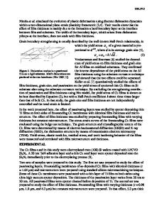
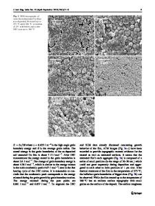
ABSTRACT A novel microtensile thin film specimen with electroplated structures is demonstrated here. It can be fitted into a specially designed microtensile apparatus which is capable of carrying out a series of tests on submicron scale thin films. Certain materials applicable in CMOS were tested here including sputtered Copper and Tantalum Nitride thin films. Copper specimens were fabricated by sputtering. For Tantalum Nitride film samples, Nitrogen gas was introduced into the chamber during the process of sputtering Tantalum films on the silicon wafer. We found the modulus of Copper and Tantalum Nitride thin films with thickness of 200 to 800nm at room temperature. The E value of Copper and Tantalum Nitride thin films tested here were consistent with the results from other measurement methods. However, the value of Tantalum Nitride thin film did not exhibit any systematic variation with respect to the thickness. INTRODUCTION Integrated circuit technologies are developing rapidly with the increasing studies on the design and fabrication of microscale systems and devices. Fabrication of integrated circuits requires placing thin films of different materials in direct contact with one another. While the primary function of these materials lies in an electrical capacity, the structural integrity of each component is essential to device performance. As IC interconnects dimension continues to diminish, the performance and reliability of aluminum alloy may soon to be replaced by copper [Vinci 1995], since copper has superior material properties such as the electrical conductivity, thermal conductivity, and high melting point than aluminum. Before copper is adopted, however, better understanding the mechanical behavior of copper thin film is necessary in order to identify its mechanical reliability concerns and to determine its differences from aluminum behavior. Tantalum Nitride (TaN) thin film has recently received extensive interest as a barrier material. According to Ranjana Saha et. al. [1997], tantalum nitride (TaN) provides superior physical properties for semiconductor barrier with respect to traditional barrier materials Titanium Nitride (TiN). As compared to TiN, the grain boundaries of TaN are often disordered while CVD-deposited TiN films typically exhibit a co-lumnar grain structure. Due to this disordered grain boundary structure, TaN may prevent copper diffusion more efficiently than TiN. In addition, it has a high melting point, good wearing resistance, highly conductivity, and thermodynamically stable with respect to metals. Numerous studies of TaN thin film had been done on its fabrication details and electrical properties [Kim et. al. 2002, Suguru et. al. 2004, Liang et. al. 2005, Chong et. al. 2005 Wang et. al. 2005], howev
Data Loading...