Residual Stress and Microstructure of Electroplated Cu Film on Different Barrier Layers
- PDF / 377,192 Bytes
- 6 Pages / 612 x 792 pts (letter) Page_size
- 60 Downloads / 308 Views
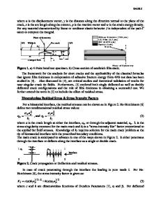
Residual Stress and Microstructure of Electroplated Cu Film on Different Barrier Layers Alex A. Volinsky1, Meike Hauschildt2, Joseph B. Vella1, N.V. Edwards1, Rich Gregory1, William W. Gerberich3 1 Motorola DigitalDNATM Labs, Process and Materials Characterization Lab, Mesa, AZ 2 University of Texas, Materials Science Lab for Interconnect and Packaging, Austin, TX 3 University of Minnesota, Dept. of Chem. Eng. and Materials Science, Minneapolis, MN ABSTRACT Copper films of different thicknesses between 0.2 and 2 microns were electroplated on adhesion-promoting TiW and Ta barrier layers on single crystal 6-inch silicon wafers. The residual stress was measured after each processing step using a wafer curvature technique employing Stoney’s equation. Large gradients in the stress distributions were found across each wafer. Controlled Cu grain growth was achieved by annealing films at 350 °C for 3 minutes in high vacuum. Annealing increased the average tensile residual stress by about 200 MPa for all the films, which is in agreement with stress-temperature cycling measurements. After aging for 1 year wafer stress mapping showed that the stress gradients in the copper films were alleviated. No stress discrepancies between the copper on Ta and TiW barrier layers could be found. However, X-ray pole figure analysis showed broad and shifted (111) texture in films on a TiW underlayer, whereas the (111) texture in Cu films on Ta is sharp and centered. INTRODUCTION The microelectronics industry is gradually moving from Al/SiO2 to Cu/lowK interconnect systems for improved performance. Currently one can buy a high-end processor from a leading semiconductor manufacturer such as Motorola that contains electroplated Cu interconnects. Although this is a tremendous achievement for the whole semiconductor industry, the continuing process of scaling requires further research and development regarding process improvements and reliability in metallization and dielectrics integration. For the process control and most reliability tests, knowledge of the thin film constitutive mechanical behavior is required. Mechanical properties of thin films often differ from those of the bulk materials. This can be partially explained by the fine-grained structure of thin films and the fact that these films are attached to a substrate. The yield stress in thin films, for example, is typically much higher than for a bulk material. However in both cases the material microstructure can have a dramatic effect on the mechanical properties. Typically for bulk materials and in some cases for thin films as well, the grain size, d can affect the yield strength in a manner described by the Hall-Petch relation:
σ YS = σ i + kd − n
(1),
where σi is some intrinsic stress, independent of the grain size d, and n is typically between 0.5 and 1. The classic 1/d0.5 Hall-Petch relationship is not typically observed for thin films due to the substrate effect, limiting thin film plasticity, or due to the dislocation looping along the metal/oxide interface, both of which st
Data Loading...