Development of Bulk GaN Crystals and Nonpolar/Semipolar Substrates by HVPE
- PDF / 566,358 Bytes
- 5 Pages / 612 x 792 pts (letter) Page_size
- 115 Downloads / 346 Views
GaN Crystals and Nonpolar/Semipolar Substrates by HVPE
Kenji Fujito, Shuichi Kubo, and Isao Fujimura Abstract The remarkable progress in nonpolar and semipolar devices based on gallium nitride (GaN) in recent years has been driven by not only advancements in the epitaxial growth technique but also improvements in the quality of bulk nonpolar and semipolar GaN substrates. At present, high-quality nonpolar/semipolar substrates are only made by slicing thick bulk GaN crystals grown by hydride vapor-phase epitaxy (HVPE). Although HVPE is currently the most successful method for obtaining high-quality bulk GaN crystals, it is still difficult to obtain uniform crystals with large diameters and thicknesses. The size of the nonpolar/semipolar substrates has been limited by the growth thickness along the c-axis of bulk GaN crystals. Here we review the growth of bulk GaN crystals by HVPE to achieve high-quality and large-sized nonpolar and semipolar substrates.
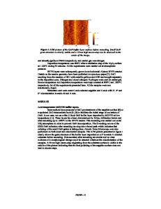
HVPE Growth of GaN Using freestanding gallium nitride (GaN) substrates has many benefits, such as low dislocation density and high thermal conductivity,1,2 for high performance device fabrication. Hydride vapor-phase epitaxy (HVPE) is currently one of the most successful and promising methods for obtaining high-quality bulk GaN substrates. In 1969, Maruska and Tirtjen reported the first GaN crystal with a thickness of approximately 50–150 µm on a sapphire substrate 2 cm2 in area grown by HVPE.3 After their pioneering work, 2-in. freestanding c-plane GaN substrates became commercially available in the early 2000s.4 One of the advantages of HVPE is its high growth rate (>100 µm/h), which is almost two orders of magnitude faster than typical vapor phase growth techniques such as metal organic chemical vapor deposition (MOCVD) and molecular beam epitaxy. The HVPE equipment is relatively simple, and it is composed of a gas supply system, heater furnace, and quartz reactor tube. Figure 1 shows a schematic drawing of a typical HVPE system.5 The technique is based on the GaN
acid (HCl), and NH3 as sources. First, HCl reacts with metallic Ga at ~800°C, forming GaCl (e.g., Equation 1). Then, GaCl flows to the growth zone to react with NH3 at ~1000°C on the substrate surface for GaN crystal growth (e.g., Equation 2). HCl(g) + Ga(l) → GaCl(g) + 1/2H2(g)
(1)
GaCl(g) + NH3(g) → GaN(s) + HCl(g) + H2(g) (2)
GaN crystals are usually grown on foreign substrates such as sapphire,3 GaAs,6 NdGaO3,7 LiGaO3,8 6H-SiC,9 or Si,10 and the substrate is subsequently removed to produce a freestanding wafer. Several removal techniques have been developed to improve productivity and process yield. The laser-induced laser liftoff technique has been used to separate GaN grown on a sapphire substrate.11,12 Oshima et al. developed the void-assisted separation method with the aid of a TiN interlayer.13 Self-separation processes using the two different thermal expansion coefficients of GaN and the foreign substrate while cooling also were developed to achieve the freestanding GaN layers.14 In the ca
Data Loading...