AlGaN/GaN Field Effect Schottky Barrier Diode for a Low Loss Switching Device
- PDF / 239,244 Bytes
- 6 Pages / 595 x 842 pts (A4) Page_size
- 15 Downloads / 311 Views
E6.3.1
AlGaN/GaN Field Effect Schottky Barrier Diode for a Low Loss Switching Device Seikoh Yoshida, Nariaki Ikeda, Jiang Li, Kohji Hataya, Takahiro Wada, and Hironari Takehara Yokohama R&D Laboratories, The Furukawa Electric Co., Ltd 2-4-3, Okano, Nishi-ku, Yokohama, 220-0073, Japan
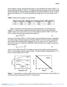
ABSTRUCT We have proposed a novel field effect Schottky barrier diode (FESBD) with a dual Schottky structure combined with an AlGaN/GaN heterostructure in order to obtain a very low on-voltage. This diode has a dual Schottky structure of a very low Schottky barrier metal and a high Schottky barrier metal for obtaining a low on-voltage. The leakage current at a reverse bias was suppressed by the pinch-off based on field effect of a higher Schottky barrier metal, resulting in increasing the reverse breakdown voltage. In this paper, we carried out a planer-type FESBD for a large current operation. The AlGaN/GaN heterostructure was grown by a metalorganic chemical vapor deposition (MOCVD). A dual Schottky structure was fabricated using Ti/Al and Pt. An ohmic electrode was also Ti/Al. As a result, the on voltage of FESBD was below 0.1 V. The reverse breakdown voltage was also over 400 V by pinch-off effect. The switching time of the diode was shorter than 3 ns. INTRODUCTION III-V nitrides have very excellent figure of merits for high-power, high-frequency, and high-temperature devices [1-5]. They are also very effective for a very low loss power switching device applications such as inverters or converters; since GaN based field effect transistors (FETs) have a very low on-state resistance. Therefore, a high efficiency inverter can be realized using GaN based FETs [6-10]. However, for realizing a high efficiency inverter, not only FETs with a low on-state resistance, but also, a freewheel diode with a very low on-voltage and a very small recovery time is required to immediately cut off the freewheeling current. The GaN is also effective for a fast recovery diode or freewheeling diode, since they have a very high switching speed, and a very low recovery charge. Recently, using an SiC, a Schottky barrier diode (SBD) with dual Schottky metal structures was proposed for realizing a low on-voltage [11, 12]. GaN based Schottky diodes with a high breakdown voltage have been also reported
E6.3.2
[13, 14]. However, there is no report for GaN SBD with a low on-state voltage. In this paper, we report on a new field effect Schottky barrier diode (FESBD) with a dual Schottky barrier structure combined with an AlGaN/GaN heterostructure. The key technology of this structure is to use a very lower Schottky barrier metal (SM1) and a higher Schottky barrier metal (SM2) for obtaining a low on-voltage and a high reverse breakdown voltage, respectively. The operation mechanism of this diode is simply introduced as shown in Fig.1 (a) and (b). When the forward bias is supplied to the FESBD, a two dimensional gas (2DEG) is the channel for current flow under the forward bias. The forward current of the diode flows from a low Schottky barrier electrode towards t
Data Loading...