Dielectric Properties of PCB Embedded Bismuth-Zinc-Niobium Films Prepared using RF Magnetron Sputtering
- PDF / 1,334,148 Bytes
- 7 Pages / 612 x 792 pts (letter) Page_size
- 51 Downloads / 381 Views
0969-W01-07
Dielectric Properties of PCB Embedded Bismuth-Zinc-Niobium Films Prepared using RF Magnetron Sputtering Seungeun Lee, Jung Won Lee, Inhyung Lee, and Yul Kyo Chung eMD Lab, Samsung Electro-Mechanics, 314,Maetan3-dong, Yeongtong-gu, Suwon, Korea, Republic of
ABSTRACT Dielectric properties of bismuth-zinc-niobium oxide (Bi1.5Zn1.0Nb1.5O7, BZN) thin films deposited by by RF magnetron sputtering have been investigated for embedded capacitor. Crystalline BZN has a pyrochlore structure in nature and shows a dielectric constant of ~ 200 with very low leakage current when crystallized. Since the process temperature is limited to < 200 due to an organic based substrate in printed circuit board, as-deposited BZN film was composed of an amorphous phase, confirmed by XRD analysis. However, it showed remarkably high dielectric constant of 113. It makes BZN to be a proper candidate as a decoupling embedded capacitor in power delivery circuits. Effects of post treatment such as oxygen plasma treatment and low temperature thermal annealing on dielectric properties of BZN thin films were studied. By optimizing deposition conditions, amorphous BZN thin film was well processed in the current printed circuit board (PCB) process and provided a capacitance density as high as 218 nF/cm2 and leakage current less than 1 µA/
㎠ at 3V.
INTRODUCTION Electronics industry is going through miniaturization of system. Therefore electronic components should be increased its integration density. In case of active components its integration density can be increased by reducing its design rule but for passive components like capacitor and resistor, it is not easy to increase the integration density because it is related with material constant like dielectric constant and resistivity. Recently embedded passive (EP) components are receiving wide interest for such miniaturization of system especially in wireless communication system [1-3]. Typically in an electronic circuit, 80% of the components are passives, which take about 50% of foot print area of the circuit board. EP technology is adopted as miniaturization solution for module solution. In addition to the size reduction, parasitic noise can be reduced by minimizing the signal and power path. Reliability also can be improved by removing solder joint of the surface mount components. Additionally, potential cost can be lessened by reducing discrete passives, quantity of fluxes and solders, and by saving the assembly cost [4]. Among the embedded passive components, capacitors are most widely studied because they are the most important components in terms of number, size and performance. There are some commercialized embedded capacitor (EC) materials of thick film type from Sanminar, 3M and Oak-Mitsui etc. Capacitance density is about 0.1~2 nF/cm2 for thick film type which is not enough for decoupling capacitor application, the typical value of 1~100 nF/cm2 for RF module applications. Thin film embedded capacitor, high capacitance density of 100~1,000 nF/cm2 and
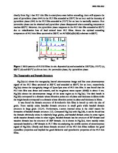
Figure 1. Schematic diagr
Data Loading...