Direct Patterning of Molecular Organic Materials and Metals Using a Micromachined Printhead
- PDF / 1,259,491 Bytes
- 7 Pages / 612 x 792 pts (letter) Page_size
- 90 Downloads / 222 Views
H1.8.1
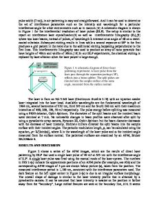
Direct Patterning of Molecular Organic Materials and Metals Using a Micromachined Printhead Jianglong Chen, Valérie Leblanc, Sung Hoon Kang, Marc A. Baldo, Paul J. Benning1, Martin A. Schmidt, and Vladimir Bulović Massachusetts Institute of Technology, Microelectronics Technology Laboratories, Cambridge, MA 02139, U.S.A. 1 Hewlett-Packard Company, Corvallis, OR 97330 U.S.A. ABSTRACT Micron-scale lateral patterning of molecular organic thin films is still one of the most challenging issues in the practical fabrication of pixelated organic light emitting device (OLED) displays. In this work we demonstrate organic and metal thin film patterning using a micromachined printhead that modulates the vapor flux of evaporated materials incident on a substrate. The printhead is integrated with an x-y-z manipulator that facilitates patterning within a vacuum environment at pressure of less than 5 × 10 −6 Torr. This printing scheme enables direct, solvent-free and mask-free patterning of organic optoelectronic devices on diverse substrates. As an example we fabricated an OLED array of 30x30 µm Alq3 (tris(8-hydroxyqunolinato) aluminum) pixels. 30 µm wide silver patterns were also directly written using the same technique. The results show that this printing method is capable of patterning molecular organic materials and metals at high resolution (800 dpi). INTRODUCTION The increasing demand for flat panel displays (FPDs) in the information technology and consumer electronics market is driving development of fluorescent/phosphorescent molecular organic light emitting devices (OLED) [1,2]. Fabrication of OLED FPDs is dependent on the throughput and yield of the constituent thin film deposition and patterning techniques. To date, the most significant challenge is in demonstration of high definition pixelated patterns and scalability of patterning techniques beyond GEN 2/3 substrate plates. A high resolution full color 17” displays require pixel width of less than 250 µm, equivalent to three 40 µm wide redgreen-blue subpixels placed side by side and spaced 40 µm apart [2]. Due to the weak intermolecular bond in organic materials, conventional semiconductor patterning methods, including photolithography and plasma processing, can damage the active organic layers leading to significant degradation in the device performance or even complete failure. Best performance molecular OLEDs are fabricated using thermal evaporation, however, defining 40 µm wide thin film patterns by vapor deposition through a shadow mask requires precise control of the shadow mask to substrate separation [3], which becomes a limiting factor when trying to scale up the mask size. Drury, et al. demonstrated that ink-jet printing can be used to generate a high definition allpolymer organic integrated circuit [4]. The inkjet printing has the advantage of precise patterning on large size substrate, but it is currently restricted to materials that can be processed in solution. It is also challenging to maintain solvent compatibility in multilayer inkjet printed
Data Loading...