Direct Synthesis of Silicon Nanowires, Silica Nanospheres, Wire-Like Nanosphere Agglomerates, and Silica-Based Nanotubes
- PDF / 1,852,158 Bytes
- 8 Pages / 612 x 792 pts (letter) Page_size
- 11 Downloads / 355 Views
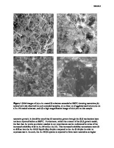
Direct Synthesis of Silicon Nanowires, Silica Nanospheres, Wire-Like Nanosphere Agglomerates, and Silica-Based Nanotubes and Nanofiber Arrays J. L. Gole,1 J. D. Stout,1 Z. R. Dai,2 and Z. L. Wang2 Schools of Physics,1 and Material Science2 Georgia Institute of Technology, Atlanta, Georgia 30332-0430 ([email protected], 404-894-4029) For several decades, the vapor-liquid-solid (VLS) process,1,2 where gold particles act as a mediating solvent on a silicon substrate, forming a molten alloy, has been applied to the generation of silicon whiskers. The diameter of the whisker is established by the diameter of the liquid alloy droplet at its tip. The VLS reaction generally leads to the growth of silicon whiskers epitaxially in the direction on single crystal silicon substrates.1-3 Recently, Lieber,4 Lee,5 Yu,6 and coworkers have extrapolated on the ideas entailed in the VLS technique to develop laser ablation of metal containing silicon targets, obtaining bulk quantities of silicon nanowires. More recently, Lee et al.5,7 have shown that oxides play a dominant role in the nucleation and growth of semiconductor nanowires be it by laser ablation, thermal evaporation, or chemical vapor deposition. Lee et al.5 have suggested a new growth mechanism, referred to as oxide assisted nanowire growth, which represents a new approach to nanowire synthesis. Our initial approach8-10 to this problem has involved the application of the techniques of high temperature synthesis to modify the approach of Lee et al. and generate virtually defect free SiO2 sheathed crystalline silicon nanowires and silica (SiO2) nanospheres which can be agglomerated to wire-like configurations impregnated with crystalline silicon nanoclusters. Further controlled condensation can extend this agglomeration to produce nanotubes and nanofiber arrays. Figures 1 correspond to Transmission Electron Micrographs of exemplary virtually uniform and straight nanowires which we have generated from a 50/50 Si/SiO2 equimolar mixture heated to a temperature of 1400oC at a total pressure of 225 Torr for 12 hours. The central crystalline silicon core is i 30 nm in diameter whereas the outer SiO2 sheathing is i 15 nm in thickness. The HRTEM views in Figures 1(b) and (c) demonstrate a number of distinguishing characteristics. Figure 1(c) demonstrates that the axes of the SiO2 clad crystalline silicon
C5.9.1
C5.9.2
nanowires are parallel to . This is distinct from the results obtained by Lee et al.5 whose wires have their axes parallel to as they display twinning, high order grain boundaries, and stacking faults. At the Si-SiO2 interface, (Fig. 1(c)), the crystal planes are best described as {211}. The wire which is depicted in Figures 1 appears virtually defect free. As figure 1(b) suggests, the inner crystalline silicon core undulates slightly. However, the fluctuations in the shading that are apparent in the HRTEM micrograph indicate that the wires are of sufficient quality that the detailed strain due to slight bending above the TEM mount can be readily observed in
Data Loading...