Dislocations and Slip Systems in V 3 Si
- PDF / 3,825,346 Bytes
- 6 Pages / 420.48 x 639 pts Page_size
- 88 Downloads / 411 Views
DISLOCATIONS AND SLIP SYSTEMS IN V3 Si
L.S. SMITH, M. AINDOW AND M.H. LORETTO IRC in Materials for High Performance Applications, and School of Metallurgy and Materials, The University of Birmingham, Edgbaston, Birmingham, B15 2TT, UK.
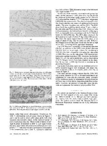
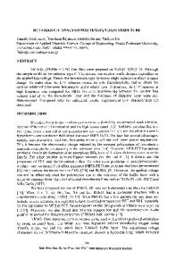
ABSTRACT A transmission electron microscopy study of the defect structure in Czochralski single crystals of V3Si is presented. As grown crystals contain occasional V5 Si 3 precipitates and a low density of edge dislocations with b = a. Following deformation to 4% strain at 1600'C in compression much higher densities of precipitates and screw dislocations are present. Images of the dislocations are doubled under certain conditions and it is suggested that this corresponds to a dissociation of the form; a =ý a/2 + CSF + a/2, as observed previously in Nb3 AI. The significance of this dissociation for deformation mechanisms in V3Si is discussed.
INTRODUCTION A great many intermetallic compounds have been considered recently as potential high temperature structural materials. The highest operating temperatures are probably offered by the "exotics" whose structures involve simple lattices with complex bases rather than those based on ordering of different species onto the sites of a simple structure. One example of such a structure is the A15 phase which is formed in certain binary systems at A3B compositions, e.g. Nb 3AI, Cr 3Si and V3 Si. As with most exotics, A15 compounds are rather brittle but the reasons for this are not well understood. In V3 Si, for example, there have been many attempts to identify the nature of defects and deformation mechanisms but no clear picture has emerged. Etch pit studies in deformed single crystals have been used to suggest that deformation occurs by slip on the systems {001) [1] and (012) [2]. Transmission electron microscopy (TEM) studies of grown-in dislocations appear to confirm that they have b = a [3] but the observation of double images [4] has caused some controversy. These features have been explained as g.b = 2 contrast [5], dipoles [6] and even pairs of dispirations on common (012) planes [7], but none of these explanations can account fully for the observed contrast. A TEM analysis of dislocation structures produced during creep deformation showed many dislocations with b = a, often arranged as arrays in subgrain boundaries [8]. The consensus would appear to be that slip must occur on the system 1001} since the lattice is simple cubic, but this has not been proved conclusively. In this paper we describe a TEM study of the dislocation microstructure in V3 Si single crystals as grown and after compression at 1600'C. The implications of these observations for deformation mechanisms in V3Si and isostructural compounds are discussed
EXPERIMENTAL PROCEDURE Single crystals of V3 Si were prepared by the Czochralski method in a tri-arc furnace with a 30g charge and using a water cooled seed rod. Compression specimens 3mm in diameter and 10mm in length were cut from the crystals using electro-discharge machining (EDM). The specimens were heated to 1
Data Loading...