Doping and crystallization of amorphous SiGe films with an excimer (KrF) laser
- PDF / 633,021 Bytes
- 5 Pages / 576 x 792 pts Page_size
- 68 Downloads / 352 Views
M. I. Chaudhryb) Department of Electrical Engineering, Center for Advanced Materials Processing, Clarkson University, Potsdam, New York 13699
S.V. Babu Department of Chemical Engineering, Center for Advanced Materials Processing, Clarkson University, Potsdam, New York 13699 (Received 28 April 1994; accepted 24 April 1995)
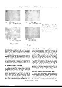
Amorphous silicon germanium (a-SiGe) films, deposited on silicon substrates at room temperature in a molecular beam epitaxy system, were transformed into a single-crystal film and doped with phosphorus by exposure to KrF laser pulses. Electron channeling patterns showed that laser exposure resulted in crystallization of the undoped a-SiGe films. The SiGe films were doped by laser irradiation, using a phosphorus spin-on-dopant. The sheet resistance of the doped films decreased with increasing numbers of pulses, reaching a value of about ~ 5 X 10⁴ ohms/D after 15 pulses. /-Vdata from mesa-type n-SiGe/p-Si diode devices were used to determine the effect of laser processing on the quality of the SiGe films.
I. INTRODUCTION Strained silicon-germanium (SiGe) films are of great technological importance due to potential applications in heterostructures devices such as high-speed bipolar devices,1 photodetectors in optoelectronic devices, and other novel optical and electronic devices.2 Polycrystalline SiGe is potentially suitable as gate material for field-effect transistors and for interconnects in devices since it is an attractive alternative to poly-Si due to its inherently lower resistivity and higher field-effect mobility.3 Conventional methods for crystallization and doping of amorphous films require high-temperature processing. Thermal annealing or ion implantation followed by hightemperature annealing is used to introduce dopants and form p-n junctions in semiconductors. Crystallization of amorphous layers also requires exposure to high temperatures. 24 Impurity contamination and degradation of minority carrier lifetime in the base region are serious problems posed by high-temperature processing.5 Laser processing offers a simple one-step method for both crystallization and doping of amorphous layers. Indeed, formation of p-n junctions on silicon by laser processing has already been reported.6"8 Laser processing offers the advantage of maintaining a low substrate temperature, while allowing instantaa) Present
address: Ultra Clean Technology, Menlo Park, California 94025. b) Present address: CHEMI Laboratories, Watervliet, New York 12189. 1884 http://journals.cambridge.org
J. Mater. Res., Vol. 10, No. 8, Aug 1995 Downloaded: 17 Mar 2015
neous local temperatures in the overlying film to be quite high.8 This process drives in surface-adsorbed dopants by a melt/regrowth step and introduces dopants without the dopant channeling tail observed in ion implantation techniques. Highly doped shallow junctions (0.1 /am) required in CMOS microfabrication have been attained by laser-induced doping of Si with boron.5 Excimer laser-induced doping of silicon by phosphorus9'10 has also been investigated. In e
Data Loading...


