Excimer Laser Crystallization of Amorphous Silicon Films for Poly-Si TFT Fabrication
- PDF / 1,060,742 Bytes
- 6 Pages / 414.72 x 648 pts Page_size
- 96 Downloads / 353 Views
of the sample and was clocked at 10 Hz. atmosphere at room temperature.
The films were crystallized in an argon
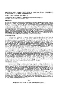
TFT Fabrication Figure 1 shows the fabrication process for an n-channel poly-Si TFT. The TFT was fabricated on a quartz substrate at low temperatures, below 6001C. A sputtered tungsten-silicide (WSi 2) layer was employed for source/drain metallization. N' poly-Si layers were prepared as source/drain regions by an ion implantation WSi2 n* poly-Si method. For the active layer, an a-Si layer was deposited by LPCVD, and it was crystallized by the XeCl excimer laser mentioned above. After annealing, the polySi film was plasma-etched to define the island pattern. A SiO 2 film was deposited as the gate insulator by LPCVD. An (A) Source-Drain Region aluminum layer was formed for gate metalization. Grain boundary passivation was accomplished by using hydrogen plasma.
L\\IZI=
ExcirnerLaser RESULTS AND DISCUSSION TFT Characteristics Figure 2 shows the Id-V. characteristics of poly-Si TFTs fabricated, with the number of laser shots ranging from 1 to 5. TFT characteristics vary dramatically between 1 and 2 shots, and only slightly after that. This is due to the fact that the first shot produces an amorphous-crystalline transition, while successive shots produce crystallinecrystalline transformations. Figure 3 shows mobilities and threshold voltages in terms of the number of shots. Mobility increases monotonically with the number of irradiations, with maximum mobility being obtained at about 20 shots. Our results indicate that film crystallinity varies with each individual irradiation step. In order better to understand the influences being exerted on TFT characteristics, we estimated the grain boundary trap densities of effective channel regions. Such density is known to be a major factor in determining those characteristics. We conducted our estimations al.'s using the theory proposed by 1) Proano et
(B) Active Layer
>SLEJm Si02
(C) Gate Insulator / Contact Hole
(D) Metallization Figure 1. Process sequence for n-channel poly-Si TFT fabrication by using excimer laser annealing.
678
Figure 2. Typical Id-Vg characteristics for poly-Si TFTs. Annealing energy density is 406 mJ/cm and number of shots is ranging from 1 to 5 shots.
l1 GATE VOLTAGE [V] 2
ENERGY DENSITY 406(mJ/cm ) 0: Mobility 0: Vth
200
S0//
E
,,
,
,
5J
*\
10 ý
0,"
r
0
0 Co
Figure 3. Electron mobility and threshold voltage for n-channel TFTs dependence on number of
ow 0 I
shots.
10
100
C,, w I-
NUMBER OF SHOTS
Figure 4 shows a plot of grain boundary trap densities in terms of the number of shots. Trap density decreases to approximately lxWl02 cm' at 20 shots, which is less than a third of that for film crystallized with only one shot. This resembles closely observed changes in mobility. The number of shots that minimizes trap density is the same as that which creates maximum mobility, i.e. mobility seems to be correlated with the grain boundary conditions.
~-1101014 E
II, /
0
/
0
SI z
LUI
a 0.
q0
ý-101
Figure 4. Gr
Data Loading...