Doping of Sub-50nm SOI Layers
- PDF / 554,246 Bytes
- 7 Pages / 612 x 792 pts (letter) Page_size
- 80 Downloads / 389 Views
1070-E04-06
Doping of Sub-50nm SOI Layers Bartek J. Pawlak1, Ray Duffy1, Mark van Dal1, Frans Voogt2, Robbert Weemaes3, Fred Roozeboom4, Peer Zalm3, Nick Bennett5, and Nick Cowern5 1 NXP-TSMC Research Center, Kapeldreef 75, Leuven, 3001, Belgium 2 NXP Semiconductors, Nijmegen, Netherlands 3 Philips, Eindhoven, Netherlands 4 NXP Semiconductors, Eindhoven, Netherlands 5 University of Newcastle, Newcastle, United Kingdom
ABSTRACT Doping of thin body Si becomes very essential topic due to increasing interest of forming source/drain regions in fully depleted planar silicon-on-isolator (SOI) devices or vertical Fin field-effect-transistors (FinFETs). To diminish the role of the short-channeleffect (SCE) control, the Si layers thicknesses target the 10 nm range. In this paper many aspects of thin Si body doping are discussed: dopant retention, implantation-related amorphization, thin body recrystallization, sheet resistance (Rs) and carrier mobility in crystalline or amorphized material, impact of the annealing ambient on Rs for various SOI thicknesses. The complexity of 3D geometry for vertical Fin and the vicinity of the extended surface have an impact on doping strategies that are significantly different than for planar bulk devices.
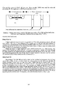
INTRODUCTION Understanding of dopant behavior in thin body Si is crucial for Fin source and drain formation. Fin tilt
As or B implantation Fin tilt C-Si
or
A-Si SOI
BOX FIN
a
BOX
b
Si substrate
Figure 1. Schematic drawings of implants into Fin (a) when source and drain is formed and of the experiment on implants into crystalline or amorphous SOI blanket wafer. (b) The tilt angle as indicated is consistent with Fin doping geometry. The a-Si layer mimics the full Fin amorphizing implant condition.
The vicinity from both sides of a large Si/SiO2 interface introduces differences from regular bulk Si doping with respect to dopant incorporation, material crystallinity, defect generation/annihilation, dopant activation, and diffusion. The study of dopant implantation in thin body Si can be conducted on SOI wafers. The sidewall implantation and diffusion in a vertical Fin can be mimicked by the tilt angle adjustment (Fig. 1) [1]. In that case the electrical and chemical analysis is simple to conduct on planar structures rather than on free standing vertical structures. The implant angles specified in the text and figure captions relate to what the process engineer would specify. The tilts specified here refer to what the sidewall would receive, thus 90-(tilt angle). e.g. 20° discussed in the figures corresponds to 90°-20°=70° received by the planar sample. – see Fig. 1b.
EXPERIMENTAL DETAILS Blanket 200 mm SOI wafers were used in the experiment. The thickness of crystalline SOI layer was controlled by etch-based thinning. Some wafers were prepared in order to mimic the fully amorphizing implant. The amorphous SOI layers were obtained by Si deposition on SiO2. The thickness of Si layers was confirmed by crosssection transmission electron microscopy (XTEM) and Rutherford backscattering
Data Loading...