Effect of Base Impurity Concentration on DC Characteristics of Double Ion Implanted 4H-SiC BJTs
- PDF / 183,055 Bytes
- 4 Pages / 612 x 792 pts (letter) Page_size
- 82 Downloads / 453 Views
1069-D07-20
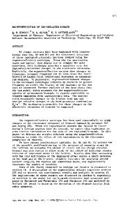
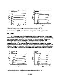
Effect of Base Impurity Concentration on DC Characteristics of Double Ion Implanted 4HSiC BJTs Taku Tajima, Satoshi Uchiumi, Kenta Tsukamoto, Kazumasa Takenaka, Masataka Satoh, and Tohru Nakamura EECE and Research Center of Ion Beam Tech., Hosei University, 3-7-2, Kajinocho, Koganei, Tokyo, 184-8584, Japan ABSTRACT Double ion implanted 4H-SiC bipolar junction transistors (BJTs) are fabricated by Al and N ion implantation to the base and emitter. The current gain of 3 is obtained at the base Al concentration of 1 x 10¹⁷ /cm3. The collector current as a function of the base Gummel number suggests that double ion implanted 4H-SiC BJT operates in the intrinsic region below the emitter in the low injection level. The high base resistance restricts the base current at VBE as low as 3 V. INTRODUCTION SiC is a promising material for ultra-low loss and high temperature devices because of high breakdown field strength and wide bandgap [1]. Many workers have studied about the device physics and processing about SiC devices such as Schottky diodes and metal-oxidesemiconductor field effect transistors (MOSFETs). Furthermore, many SiC bipolar junction transistors (BJTs), which are expected to be high temperature devices, have been fabricated using epitaxial layers, grown on SiC substrate [2,3]. In the fabrication process of SiC BJT, the ion implantation is only used to form p+ contact region to the base because the ion implantation would be unsuitable to form pn junctions of base-emitter and base-collector. Indeed, it has been reported that SiC BJT with ion-implanted emitter shows the current gain less than 1, which is attributed to a low minority carrier life-time in the base-emitter space charge region [4]. In recent, however, the novel annealing system has been developed for the post ion implantation of SiC [5]. We have reported that Al ion implanted p+n junction diode shows the excellent I-V characteristics with the diffusion current, which was annealed at 1900 oC using electron bombardment annealing system (EBAS, Canon-ANELVA) [6]. It is therefore expected that SiC BJT is fabricated using ion implantation techniques combined with the novel annealing technique. In this study, we investigate the dependence of base impurity concentration on dc characteristics for the double ion implanted 4H-SiC BJT, in which ion implantation is used to form both the base and emitter regions.
EXPERIMENTAL DETAILS Device structure
Figure 1. Structure of the fabricated double ion implanted 4H-SiC BJT.
Figure 2. The doping profiles of the base, emitter, and p+ regions
Figure 1 schematically illustrates the structure of fabricated double ion implanted 4H-SiC BJT. The depth of i ntrinsic base is 0.3 µm. The width (WE) and length (LE) of the emitter were 90 and 100 µm, respectively. The p+ contact region to the base with a width of 6 and a depth of 0.6µm is formed surrounding the emitter with a spacing of 20 µm. Figure 2 shows the do ping profiles of the base, emitter, and p+ regions, which are calculated by using the stopping and ra
Data Loading...