p-GaAs Base Regrowth for GaN HBTs and BJTs
- PDF / 62,857 Bytes
- 6 Pages / 612 x 792 pts (letter) Page_size
- 60 Downloads / 339 Views
p-GaAs BASE REGROWTH FOR GaN HBTs AND BJTs G. Dang1, A.P. Zhang1, X.A. Cao2, F. Ren1, S.J. Pearton2, H. Cho2, W.S. Hobson3, J. Lopata3, J.M. van Hove4, J.J. Klaassen4, C.J. Polley4, A.M. Wowchack4, P.P. Chow4, D.J. King4 1
University of Florida, Department of Chemical Engineering, Gainesville, FL 32611 University of Florida, Department Materials Science and Engineering, Gainesville, FL 32611 3 Bell Labs, Lucent Technologies, Murray Hill, NJ 07974 4 SVT Associates, Eden Prairie, MN 55344 2
ABSTRACT Low resistance ohmic contacts are difficult to form to p-type GaN and AlGaN due to the unavailability of growth methods for highly p-doped GaN and AlGaN. A p-type carbon-doped GaAs regrowth on p-GaN prior to ohmic metallization has been shown in previous work to improve contact resistance to p-GaN [13]. Applying the regrowth method to the p-base regions of npn structured bipolar transistors, AlGaN/GaN heterojunction bipolar transistors and GaN bipolar junction transistors have been demonstrated. GaN/AlGaN epilayers were grown with a molecular beam epitaxy system. Highly carbon-doped p-GaAs (1020 cm-3) was regrown on the devices (~500 Å) in the base contact region by metal organic chemical vapor deposition after emitter mesa etching. Emitter and base mesa structures were formed by Inductively Coupled Plasma etching under low damage conditions with a Cl2/Ar chemistry. SiO2 was used for emitter sidewall formation to reduce leakage current to the emitter, as well as for a mask for GaAs base regrowth. Very high current densities were obtained for common base operation in both device types. The devices were operable at 250 ºC. INTRODUCTION AlGaN/GaN-based devices have proven to be significant in high temperature and highpower semiconductor device applications. An assortment of devices based on this material system, including high breakdown power diodes, MOSFETs, and HEMTs, have been demonstrated to be operable at high temperatures and high powers [1-8]. Recently, there has been steady progress in the advancement of AlGaN/GaN heterojunction bipolar transistors (HBTs) and bipolar junction transistors (BJTs) [9-12]. HBTs and BJTs are desired for potential applications in satellite and radar communications, which would require operation in the 1-5 GHz range, under temperatures greater than 400 °C, and with powers greater than 100 W. One area under intense research, is the improvement of contact resistance to p-GaN. It has been shown previously that a heavily carbon-doped p-GaAs regrowth on p-GaN will improve contact resistance [13]. High contact resistance creates heating in the device and will demand more power for device operation. In this paper, we use this regrowth method to create p-base contacts to HBT and BJT npn structures and report on their dc characteristics at temperatures up to 250 °C.
T6.13.1
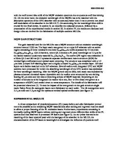
Figure 1. HBT, BJT growth structures and fabricated device cross-sections. EXPERIMENTAL DETAILS Fig. 1 shows the epitaxial growth structures as well as fabricated device structures for the HBTs and BJTs. The structures were g
Data Loading...