Effect of SP 3 /( SP 2 + SP 3 ) Carbon Fraction on the Photoelectric Threshold and Electron Affinity of Diamond Films
- PDF / 993,381 Bytes
- 5 Pages / 414.72 x 648 pts Page_size
- 98 Downloads / 347 Views
irnSCC 1.4 SCCM 0.2SCCM
S0.9 SCCM
600
12oo
1800
Raman Shift ( cm)
Figure 1. SEM photographs of CVD diamond films grown using methane flow rates of 0.6 sccm, 0.9 sccm, 1.2 sccm and 1.4 sccm. The inset shows the Raman spectra of the films.
sccm to 1.60 sccm. In order to grow a conducting film, diborane was introduced in concentrations of 1 ppm relative to hydrogen resulting in p-type films. The growth procedure was terminated by first shutting off the methane flow while maintaining the sample, filament, and H2 settings for 2 minutes. Then the filament, sample heater and H 2 flow were turned off in that order. The Raman measurements were made using the 5145 A line of an argon ion laser. The XPS measurements were made using a VG ESCALAB Mark II system with an energy resolution of 0.08 eV in a vacuum < 10`° Tort. The photoelectric threshold measurements were made using a 150 W Xenon lamp and grating monochromator. The photoelectrons were collected using a tungsten wire grid positioned approximately 2 mm above the sample, and the photocurrent was measured using modulation techniques and a lock-in amplifier. RESULTS AND DISCUSSION SEM images of films grown using methane flow rates of 0.6 sccm, 0.9 sccm, 1.2 sccm, and 1.4 sccm are shown in Fig. 1. We observe that, as the methane flow rate increases, the crystallite size decreases and the number of grain boundaries between crystallites increases. Raman spectra of these films are shown in the inset in Fig. 1. The Raman spectra show a sharp peak at 1332 cmto single crystal diamond. As the methane flow rate increases, the intensity of the diamond peak at 1332 cm' decreases relative to the intensity of peaks due to sp2 and disordered carbon. A broad peak at 1150 cm-1 is due to disordered or nanocrystalline diamond; a peak at 1350 cm' to disordered or nanocrystalline graphite; a peak at 1527 cm-' to sp3-sp2 carbon networks; and, a peak at 1579 cm-' to crystalline graphite [4]. It has been reported that the sp2 and sjp-sp2 carbon networks exist mainly at the grain boundaries [5]. Raman spectroscopy is good for qualitative analysis. Since the diamond films are transparent, Raman spectroscopy also gives information about the bulk of the film. However, it is not possible to obtain a quantitative characterization of
138
XPS of Carbon 1ce P,,l,-
14 ccmL-c
4-0
290
c
3
-
1
sJccm
289
288
287
286
285
284
283
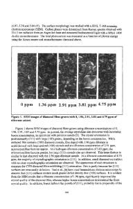
Binding Energy (eV) Figure 2. X-ray photoelectron spectroscopy data of the C Is line for diamond films grown using methane flow rates of 0.6 sccm, 0.9 sccm, 1.2 sccm and 1.4 sccm. Curves are offset for clarity. the fraction of sp3 carbon from the Raman data because the probability for Raman scattering from sp2 carbon is on the order of 50 times greater than that from sp3 carbon [4]. To obtain a quantitative characterization of the fraction of sp3 carbon at the surface of the films, we used the technique reported by Waite and Shah [6] involving XPS of the C Is line. Survey XPS spectra of the films showed no detectable oxygen or other adsorbates. Figure 2 shows
Data Loading...