Effect of the annealing treatments on the transport and electroluminescence properties of SiO 2 layers doped with Er and
- PDF / 449,067 Bytes
- 7 Pages / 612 x 792 pts (letter) Page_size
- 19 Downloads / 378 Views
Effect of the annealing treatments on the transport and electroluminescence properties of SiO2 layers doped with Er and Si nanoclusters. O. Jambois1, J.M Ramirez1, Y. Berencen1, D. Navarro-Urrios1, S. Hernández1, A. Anopchenko2, A. Marconi2, N. Prtljaga2, N. Daldosso2, L. Pavesi2, J.-P. Colonna3, J.-M. Fedeli3 and B. Garrido1 1
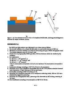
Departament d'Electrònica, Universitat de Barcelona, Carrer Martì i Franquès 1, Barcelona 08028, Spain 2 Nanoscience Laboratory, Department of Physics, University of Trento, Via Sommarive 14, Povo (Trento) 38123, Italy 3 CEA,LETI, Minatec 17 rue des Martyrs, 38054 Grenoble cedex 9, France ABSTRACT We studied the effect of RTP and furnace annealing on the transport properties and electroluminescence of Si-nc embedded in SiO2 layers, and of Er ions coupled to Si-nc. The light emitting devices have been fabricated in a CMOS line by implantation of Si and Er in SiO2. The results show that for the same annealing temperature, furnace annealing decreases electrical conductivity and increases probability of impact excitation, which leads to an improved external quantum efficiency. Correlations between phenomenological transport models, annealing regimes, and erbium electroluminescence are observed and discussed. INTRODUCTION For several years, silicon-based photonic devices have been widely considered in order to develop integrated circuits allowing to overcome the microelectronic bottlenecks. The challenge for silicon photonics is to manufacture low-cost information processing components by using standard and mature CMOS technology. Numerous photonic devices have already been developed in the last years for light propagation, modulation or detection on silicon substrates. The ultimate goal for the photonic and electronic convergence would be to monolithically integrate powerful Si-based light sources into the CMOS photonic integrated circuits. Some encouraging works have reported the possibility to obtain efficient Si-based light emitting diodes [1, 2, 3]. The use of Si nanoclusters (Si-nc) as sensitizers for Er ions luminescence has been demonstrated as promising for telecom applications, in particular to achieve an injection Si-based laser, but some efforts have still to be pursued in order to optimize the Er fraction coupled to Si-nc and improve the injection properties [4, 5]. In this work we report the study of charges injection and transport in SiO2 layers doped with Si-nc and Er ions. First, layers free of Er are studied in order to understand the role of the annealing on the transport and on the EL excitation. Then, a layer were Er has been incorporated is studied. The origin of the Er electroluminescence, by direct excitation or by transfer from Sinc is addressed. EXPERIMENT The layers are 50 nm thick silicon rich silicon oxides made by Si implantation in a SiO2 layer grown by LPCVD. Two different Si excess have been introduced by varying the dose of
implantation. Measurements made by X-ray photon spectroscopy (XPS) show that the layers with the lower Si excess have 9 at.% excess, wherea
Data Loading...