Effect of the Introduction of a MBE Buffer Layer on the Morphology of InSb Almbe Layers Grown on InP Substrates
- PDF / 3,092,867 Bytes
- 6 Pages / 414.72 x 648 pts Page_size
- 74 Downloads / 334 Views
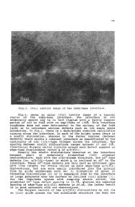
ABSTRACT In this paper we report on the morphology of InSb layers grown by atomic layer molecular beam epitaxy (ALMBE) onto InP substrates at low temperatures (330 parallel to the interface. Some of these dislocations are marked with arrows in figure 6. The average distance between two contiguous dislocations was found to be =4.4nm, which is close to the value we should have for a complete strain relaxation, according to the maximum initial mismatch of 10.4%. This result is similar for the rest of 477
the samples which also presented a fully relaxed InSb layer. In order to explain the dislocation nucleation mechanism, we refer to that proposed by C.J.Kiely et al.[3] for InSb relaxation on GaAs for edge-type dislocations. Since the first stages of InSb growth are via island nucleation, they grow coherently until they reach a critical size along < 110 > directions. This size is the same than the dislocation separation. Then the dislocation formation is energetically favoured due to the increasing strain as the islands become larger. Then two mechanisms for dislocation nucleation are proposed: (1) by dislocation formation at the island edge and propagation through the centre; and (2) by the formation of the line defect at the periphery of the island. CONCLUSIONS In summary, by Transmission Electron Microscopy and Micro Raman Spectroscopy we have analyzed the crystalline morphology of InSb layers grown by ALMBE on (001) InP substrates. The growth of an intermediate MBE InSb/InP buffer layer leads to an anomalous growth that introduces complex three-dimensional defects consisting in the association of four twins on the {111 planes. We have find two types of these structures: one leading to a pyramid in the top surface of the epilayer due to the change in crystal orientation inside the region bordered by the four E3 boundaries; and a second exhibiting a truncated pyramid owing to the recovering of the original crystal orientation at the interface between the InSbMBE and InSb-ALMBE buffer layers. The InSb epilayers grown by ALMBE at lower temperature without buffer layer presented the higher crystalline quality. In all the cases the systems were fully relaxed by a perfect network of pure-edge misfit dislocations at the interface. ACKNOWLEDGMENTS This work was funded by the Spanish CICYT program MAT95-0966. REFERENCES 1. Y. Sugiyama, Y. Nakata, K. Imura, S. Muto and N. Yokoyama, Extended Abstracts of the 1995 International Conference on Solid State Devices and Materials, Osaka, 1995, pp.773-775 2. G.M. Williams, A.G. Cullis, C.F. McConville, C.R. Withehouse and P.W. Smith, Inst. Phys. Conf. Ser. 100, 205 (1989). 3. C.J. Kiely, J-I. Chyi, A. Rockett and H. Morkoq, PhilosophicalMagazine A, 60, 321, (1989). 4. J.E. Oh, P.K. Bhattacharya, Y.C. Chen and S. Tsukamoto. J. Appl. Phys. 66, 3618, (1989). 5. S.D. Parker, R.L. Williams, R. Droopad, R.A. Stradling, K.W.J. Barnham, S.N. Holmes, J. Laverty, C.C. Phillips, E. Skuras, R. Thomas, X. Zhang, A. Staton-Bevan, D.W. Pashley, Semicond. Sci. Technol. 4, 663 (1989). 6. T. Utzmeie
Data Loading...


