High Resolution Electron Microscopy Studies of MBE Grown InSb Layers on GaAs (100)
- PDF / 3,710,394 Bytes
- 6 Pages / 420.48 x 639 pts Page_size
- 94 Downloads / 370 Views
HIGH RESOLUTION ELECTRON MICROSCOPY STUDIES OF MBE GROWN InSb LAYERS ON GaAs (100). C.J.KIELY, J-I.CHYI, A.ROCKETT AND H.MORKOc. Co-ordinated Science Laboratory, University Urbana-Champaign, Urbana, IL. 61801, USA.
of
Illinois
at
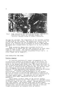
ABSTRACT InSb films grown directly on (100) GaAs substrates by MBE have been examined in the transmission electron microscope. High quality, epitaxial layers were deposited despite the 14.6% lattice mismatch between film and substrate. Nearly all of the misfit strain has been accommodated by a square array of a/2(011) edge-type misfit dislocations spaced on average 29A apart. These defects are proposed to be spontaneously generated in the epitaxial layer almost as soon as it begins to grow, and are favoured over 600 type dislocations because they are more efficient at relieving misfit strain while allowing more coherent interface area to form. The films that have been produced have low defect densities (ie. threading dislocations and microtwins) considering the large lattice mismatch in this system. Antimony precipitates have been noted in some films, but can be totally eliminated by careful control of the In/Sb flux ratio. Finally we have observed that loss of Sb from the specimen surface leads to a gradual degradation of the InSb during TEM observation, leading to the appearance of surface indium or indium oxide. INTRODUCTION The III-V semiconductor InSb with its very low bandgap (0.165eV) is a suitable material for infrared source and detector applications. Recently, there have been several efforts to grow epitaxial InSb layers directly onto semi-insulating GaAs substrates (14.6% mismatch) by a variety if techniques such as metal organic vapour phase epitaxy [1], metal organic magnetron sputtering [2] and molecular beam epitaxy [3-5]. The potential advantage of growing the detector material directly on a GaAs substrate is that signal processing could then be integrated with the detector on a single substrate chip, which would lead to significant gains in device performance. Only very limited TEM studies of the InSb/GaAs system have been reported [3,5]. In this paper we present an in-depth characterisation of the highly mismatched InSb/GaAs heterointerface by conventional TEM and high resolution electron microscopy (HREM). In particular, the interfacial and misfit dislocation structures are analysed and a mechanism for misfit dislocation formation is proposed. The most commonly observed types of growth defects are identified and various methods for reducing the overall defect density are discussed. Finally, results on the extent of electron beam damage of InSb layers occurring during TEM observation are presented. EXPERIMENTAL Details of the growth conditions for and subsequent electrical characterisation of our MBE InSb/GaAs samples have been reported elsewhere [4] and will only be outlined very Mat. Res. Soc. Symp. Proc. Vol. 139. "1989 Materials Research Society
118
briefly here. The InSb layers were grown in a Riber MBE system equipped with crackers to reduce the evaporated As
Data Loading...